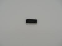
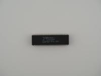
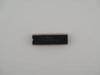
Holding this piece of computing history, the first thing I notice is the stark utilitarianism of the early 1980s IC design. We are looking at a classic 16-pin dual in-line package, molded in standard matte black plastic epoxy resin. The tin-plated pins show mild oxidation and scuffing, typical of a chip that has been socketed, pulled, and tossed into a parts bin over the decades. Placing it on the scale confirms it weighs exactly 1.0 gram, and the ruler shows it spanning roughly 19mm in length.
Right on the top surface, the laser etching is faint but highly readable under the right light, featuring the unmistakable Texas Instruments logo with the outline of the state of Texas.
TMS4164-15NLJ
6XB Δ 8441 18
This artifact is not some multi-thousand dollar ceramic mainframe processor studded with gold pins. It is a mass-produced jellybean part. But do not let the cheap plastic fool you. Chips exactly like this one built the foundation of the home microcomputer revolution.
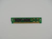
The TMS4164 is a 65,536-word by 1-bit Dynamic Random Access Memory chip. In plain terms, it holds 64 Kilobits of data. To give a machine 64 Kilobytes of usable RAM, you had to wire up a bank of eight of these chips in parallel so each one could handle a single bit of the 8-bit data byte. IBM required a ninth chip in the bank just for parity checking.
What makes the 4164 architecture a heavy metal engineering milestone is its power delivery. Its predecessor, the notorious 4116 DRAM, was a nightmare to work with because it required three separate power voltages: +5V, -5V, and +12V. If those voltages did not sequence perfectly during boot, the chip would literally cook itself. Texas Instruments and other fabricators engineered the 4164 to run on a single +5V supply. This single-voltage operation drastically simplified motherboard designs, reduced thermal output, and allowed system builders to pack massive amounts of memory into tight spaces.
The -15 suffix denotes an access time of 150 nanoseconds. By 1984 standards, this was right in the sweet spot for consumer performance, perfectly matching the bus speeds of the popular processors of the era. The chip uses a multiplexed addressing scheme, feeding the 16-bit address into the chip in two 8-bit chunks down the same pins to keep the package size restricted to just 16 pins.
This is the unsung blue-collar worker of the vintage computing world. The CPUs get all the glory. People worship the MOS 6502 and the Intel 8088. But those processors were absolutely starved for data without rows upon rows of these black plastic rectangles flanking them on the logic board.
The 4164 DRAM was the beating heart of the Commodore 64, the Apple IIe, and the original IBM PC 5150 motherboards. When you fired up an early 80s machine and saw the RAM count tick up on a monochrome monitor, you were watching an army of these exact ICs waking up and refreshing their tiny internal capacitors.
There is a fantastic bit of hardware lore regarding how frequently DRAM chips of this era failed. Because dynamic memory stores data in microscopic capacitors that constantly leak charge, a single bad cell would crash the whole machine. Vintage repair techs developed a legendary brute-force diagnostic trick known as "piggybacking." If a computer was failing memory tests, a technician would literally force a known-good 4164 directly on top of a suspected bad chip on the motherboard, pressing pin-to-pin. If the system suddenly booted, you knew exactly which chip to desolder and replace.
Identifying this artifact is straightforward, as the part numbering scheme from Texas Instruments is incredibly well documented.
The TMS prefix is the standard Texas Instruments semiconductor identifier. 4164 signifies the 64Kx1 DRAM industry standard architecture. The -15 explicitly confirms the 150ns speed grade.
The second line gives us the precise birthdate of this specific unit. The 8441 string is a standard EIA date code. This chip rolled off the manufacturing line in the 41st week of 1984. This timing places it right at the absolute zenith of the 8-bit home computing boom, just before the industry fully pivoted to denser 256k memory chips. The NLJ suffix points to the specific plastic DIP packaging formulation TI used at that fabrication plant.
It is a remarkably clean, intact specimen of the memory that defined a generation.