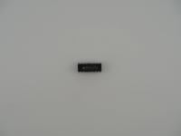
Holding this piece of computing history in the lab, I am immediately drawn to the physical footprint. Placing it on the scale, it registers a mere 1.5 grams. Measuring it against the ruler, it spans roughly 26 millimeters. It is a dense, unassuming block of black epoxy resin, but rotating it to view the bottom reveals its defining characteristic.
The pins do not point straight down in two parallel rows. Instead, we have a continuous line of twenty legs alternating left and right in a staggered formation. Looking closely under the lights, the pins on this specific unit are in remarkably pristine condition with zero visible bending or stress fractures at the brazing points.
The surface laser etching is perfectly legible, providing us with the exact forensic data we need:
TOSHIBA 1123HCK
TC514400AZ-60 JAPAN
The molding is highly standard for the era, featuring a distinct, deep circular dimple on the left side to indicate pin 1. The micro-texture of the plastic is matte, designed to withstand the ambient heat of a densely packed circuit board without blistering.
Diving into the silicon beneath the plastic, this is a 4-Megabit Fast Page Mode (FPM) Dynamic RAM chip. The architecture is organized as $1,048,576$ words by 4 bits. When you do the math, that translates to exactly 512 Kilobytes of storage per chip. To get a full 4 Megabytes of RAM, an engineer would need a bank of eight of these ICs.
The -60 suffix is where the performance metrics get interesting. This indicates an access time of 60 nanoseconds. In the early 1990s, a 60ns rating was absolutely screaming fast. Standard memory of the time hovered around 80ns to 100ns. Builders needed 60ns silicon to run high-end 386DX and 486 systems without introducing crippling wait states in the BIOS.
The packaging itself is an engineering workaround. The ZIP (Zig-zag Inline Package) was deployed to solve a spatial crisis on motherboards. Traditional Dual Inline Packages (DIP) took up too much horizontal surface area. By using a ZIP form factor, engineers could stand the memory chips vertically on their edge. The staggered pins allowed the traces on the PCB to route cleanly without shorting, effectively doubling the density of memory you could cram into a single square inch of fiberglass.
To hold a Toshiba memory chip from this era is to hold a relic of the great DRAM wars. In the late 1980s and early 1990s, Japanese fabricators like Toshiba, NEC, and Hitachi completely dominated the global memory market. They perfected high-yield, high-density fabrication techniques that American companies initially struggled to match.
The ZIP package has a massive cult following, primarily built on a foundation of pain. If you were upgrading a Commodore Amiga 3000, a high-end caching hard drive controller, or a premium SVGA video card, you lived in fear of the ZIP socket. Installing these required perfectly parallel pressure. If your finger slipped, or if you pushed at a slight angle, the incredibly flimsy legs would fold flat against the package. Bending them back using a mechanical pencil or tweezers often resulted in a snapped pin, instantly destroying an expensive piece of silicon.
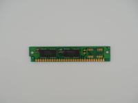
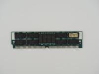
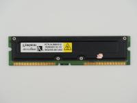
There is a myth among some younger hardware enthusiasts that SIMMs (Single Inline Memory Modules) completely replaced individual memory ICs overnight. This chip proves otherwise. Even as memory modules became popular, raw ZIP chips like this remained the standard for expanding VRAM on graphics cards and populating proprietary expansion boards where vertical clearance was an asset.
Based on the surface text and historical context, the provenance of this artifact is highly clear to me. The date code 1123HCK tells a distinct story. The leading '1' points to the year 1991, and '123' specifies the 23rd week of that year. This places the manufacturing date squarely in June of 1991, which aligns perfectly with the market explosion of 4-Megabit densities.
The part number syntax TC514400AZ breaks down logically under Toshiba's internal cataloging system. The TC is their standard prefix for semiconductor logic and memory. 514400 identifies the 1M x 4-bit FPM DRAM structure. The A denotes the specific die revision, meaning Toshiba had already refined and optimized the original silicon layout to improve yields. Finally, the Z explicitly dictates the Zig-zag Inline Package form factor.
This piece is a perfect time capsule from the exact moment when megabytes started replacing kilobytes in the common consumer vocabulary.