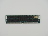
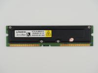
Weighing in at a mere 4.2 grams and stretching just under 90mm across the ruler, this specific unit is a masterclass in stripped-down utility.
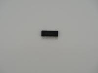
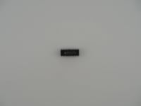
Looking closely at the surface under good lighting, the markings are incredibly crisp. We have two identical surface-mount memory packages dominating the top side of the PCB. Here is exactly what is laser-etched into the black epoxy:
TOSHIBATC514400AFT-80
JAPAN 9333HCK
The PCB itself is a standard two-layer affair, sporting a vibrant green solder mask with the trace routing highly visible. Faint gold flashes from the test points and the 30-pin edge connector reveal very little wear, meaning this artifact was not subjected to the endless insertion and removal cycles that usually strip the plating off these old modules. Stamped right onto the board are the identifiers 1M03 and the number 30 near the right edge, confirming its pin count. It is a humble, utilitarian piece, but it represents the exact threshold where personal computing started demanding serious memory footprints.
Let us tear down the math and silicon of this artifact. This is a 1 Megabyte, 30-pin Single In-line Memory Module.
The brains of the operation are the two Toshiba TC514400AFT-80 chips. Decoding Toshiba's silicon nomenclature tells us exactly what we are dealing with. The "51" indicates a dynamic RAM component. The "4400" designates the architecture as a 4-Megabit Fast Page Mode (FPM) DRAM, internally organized as 1,048,576 words by 4 bits.
Because a 30-pin SIMM requires an 8-bit wide data bus to talk to the motherboard, a single 4-bit chip cannot do the job alone. You need two of them operating in tandem to provide the full 8-bit width. Therefore, two 1Mx4-bit chips give us exactly 1 Megabyte of usable capacity. Notice the empty solder pads on the PCB? There is no third chip populated here. That missing third chip would have been a 1Mx1-bit DRAM used for parity checking. Since it is absent, we can definitively categorize this artifact as a non-parity memory module.
The -80 suffix is the speed grade, meaning this silicon has an 80-nanosecond row access time. In the early 90s, 80ns was standard, acceptable performance for a 33MHz or 40MHz system. If you were pushing a high-end 486DX2-66, you really wanted to hunt down the much faster 70ns or 60ns variants to avoid bottlenecking your screamingly fast CPU with wait states. The physical packaging of the chips is TSOP (Thin Small Outline Package), a massive space-saving upgrade over the bulky SOJ (Small Outline J-lead) packages that dominated the earlier 256KB modules.
You cannot talk about 30-pin SIMMs without talking about the sheer physical geometry of building a PC in 1993. Because a 386 or 486 processor utilized a 32-bit memory bus, and each of these 30-pin SIMMs only provided an 8-bit bus, you could never just install one stick. You had to install them in perfectly matched banks of four. Upgrading your rig meant buying four of these 1MB sticks at a time just to get 4MB of total system RAM. Mismatching the speeds (mixing 80ns with 70ns) or mixing parity with non-parity was a guaranteed recipe for blue screens and system lockups.
There is an incredible historical anomaly tied to this exact artifact. Check the date code: 9333. That means these chips were packaged in the 33rd week of 1993, which places production in mid-August.
On July 4, 1993, an explosion obliterated the Sumitomo Chemical plant in Niihama, Japan. That single factory produced over 60 percent of the world's cresol novolac epoxy resin, the exact black plastic used to encapsulate silicon chips like the ones on this module. The resulting global panic caused RAM prices to absolutely skyrocket overnight. Memory prices tripled, and people were literally stealing SIMMs out of display computers at retail stores. This specific Toshiba module rolled off the assembly line right in the dead center of the great 1993 RAM crisis. It is a survivor of one of the most volatile eras in semiconductor manufacturing history.
Identifying this artifact was a straightforward, deeply satisfying process. The sheer volume of 30-pin SIMMs manufactured means the documentation is remarkably well-preserved in the vintage computing community.
The visual evidence is undeniable. The physical 30-pin edge connector instantly locks it into the late 286 to early 486 era. The lack of a third parity chip immediately classifies it as an 8-bit non-parity stick. By referencing Toshiba's legacy semiconductor databooks, the TC514400 part number perfectly aligns with 1Mx4 Fast Page Mode DRAM. The math is absolute.
Furthermore, the board layout, utilizing the high-density TSOP packages rather than older DIP or SOJ, aligns perfectly with the 1993 manufacturing date. Earlier 1MB modules often required eight or nine separate 1-Megabit chips crammed onto a taller PCB. This module represents the mature, highly optimized tail-end of the 30-pin SIMM lifecycle just before the industry aggressively pivoted to the longer 72-pin standard for Pentium systems.