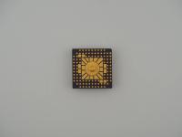
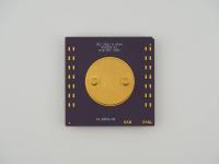
Clocking in at exactly 10.5 grams on the scale, this 1.1-inch square package feels like a tiny, gold-plated brick of pure Cold War-era engineering.
Looking at the bottom of the artifact, we have a beautiful, flawless gold cap bonded to a deep purple ceramic substrate. The laser etching is crisp and perfectly legible:
[National Semiconductor "Squiggly N" Logo]
F9306
BC1205DJQN
The ceramic itself has that classic, slightly porous matte texture that absorbs light, which makes the highly reflective gold cap and pins pop perfectly in contrast. Counting the grid, we are looking at a 72-pin dual-concentric square array. The outer ring consists of 40 pins, and the inner ring holds 32. The brazing on the pins is immaculate. You can see the tiny, precise fillets of solder holding each gold pin to the ceramic substrate.
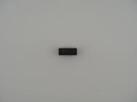
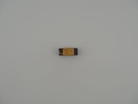
But the real showstopper is the top side. Flipping this specific unit over reveals a thick gold heat spreader plate featuring two brutally utilitarian threaded studs. This is not a chip designed for passive airflow. This is a chip designed to have a massive piece of aluminum or copper bolted directly to its skull.
When you see threaded studs on a ceramic package from the early 1990s, you are almost always looking at ECL (Emitter-Coupled Logic) or a very high-power BiCMOS gate array.
Standard CMOS logic of this era ran relatively cool. ECL, however, ran blistering hot because its transistors were always kept in an active state to eliminate turn-on delay. The trade-off for this massive thermal penalty was raw, unadulterated speed. To keep the silicon die from melting its own package, engineers had to design physical mounting systems to clamp heatsinks down with extreme mechanical pressure. Those two threaded studs aren't just for show. They ensure perfect, high-pressure mating between the internal gold heat spreader and the external cooling solution.
The CPGA-72 (Ceramic Pin Grid Array) package itself is a masterclass in high-reliability packaging. The gold plating prevents oxidation, ensuring perfect electrical contact over decades, while the dense ceramic provides a stable thermal expansion coefficient that prevents the internal wire bonds from shearing when the chip rapidly heats up and cools down.
In the late 1980s and early 1990s, before x86 completely consumed the world, heavy iron was built differently. If you were building a supercomputer, a high-end mainframe, or advanced military avionics, you did not use off-the-shelf processors. You used arrays of custom ASICs (Application-Specific Integrated Circuits) to build your logic boards.
National Semiconductor was a massive player in this space. While they are famous for their 32000-series microprocessors, their true bread and butter was providing the glue logic, gate arrays, and custom silicon that made massive supercomputers tick. A common myth in vintage computing is that microprocessors killed custom logic overnight. The reality is much messier. Chips like this BC1205DJQN represent the stubborn, high-performance holdouts of the custom silicon era. They were expensive to design, hot, power-hungry, and incredibly fast.
This artifact is a genuine mystery, and that is exactly why I love having it in my collection. Let us break down the surface text.
The logo is undeniably National Semiconductor. The top line, F9306, is almost certainly a date code. It tells us this chip rolled off the fabrication line in the 6th week of 1993. The F prefix is fascinating. National Semiconductor acquired Fairchild Semiconductor in 1987. It is highly probable that the F denotes a former Fairchild fabrication plant (like the famous facility in South Portland, Maine) that was retained by National Semi for high-reliability military and industrial runs.
The primary part number, BC1205DJQN, requires some educated deduction. The BC prefix in National Semiconductor parlance typically stands for Bipolar Custom or BiCMOS Custom logic. The 1205 designates the specific customer design or gate count. The suffix DJQN is a classic military/aerospace packaging code. The D often denotes a ceramic package, while J, Q, and N are standard markers for high-reliability screening, military temperature range ratings, and specific burn-in testing protocols.
While I cannot point to the exact radar system, mainframe, or telecommunications switch this specific unit was designed for, the physical evidence tells a complete story. The threaded studs, the heavy gold plating, the ceramic substrate, and the military-style part number all point to a high-power, high-reliability custom logic chip built for a very serious piece of heavy iron.