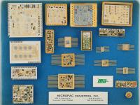
Here we have a truly beautiful and enigmatic set of components from my collection. Looking through this small acrylic case, I am immediately struck by the sheer amount of gold. These are classic military and aerospace flat-pack integrated circuits and hybrid modules.
Because many of these specific units are either decapped, uncapped prototypes, or stripped down to their bare lead frames, the traditional top-side identifying text is entirely absent. If they were fully stamped for military procurement, the ceramic lids would typically bear markings similar to: MICROPAC IND M38510/ 883B
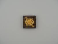
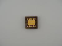
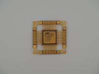
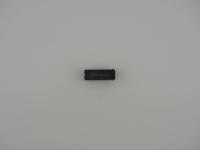
Holding these pieces and looking closely at the macro details, the craftsmanship is staggering. The ruler in the frame shows just how tiny these bodies are, measuring roughly a quarter of an inch across. The leads are long, flat ribbons of heavily gold-plated Kovar. Some of the artifacts here are completely bare ceramic substrates with intricate gold traces waiting for silicon. Others have bright white alumina ceramic lids.
The standout piece for me is the open-cavity unit with the complex hybrid layout. Peering into that tiny square, you can clearly see bare semiconductor dies, thick-film resistors, and miniature surface-mount capacitors all wire-bonded together in a beautifully chaotic microscopic city. The aesthetic "cool factor" is off the charts. This is the heavy metal of the 1960s space race.
To understand why these look the way they do, we have to talk about surviving the apocalypse. Or at the very least, surviving a rocket launch.
The flat-pack form factor was originally invented specifically for the military in the early 1960s. Standard through-hole components like the dual in-line package (DIP) were too bulky and their pins were highly susceptible to breaking under extreme vibration. The flat-pack solved this. By laying the gold ribbon leads flat against a printed circuit board and spot-welding or surface-soldering them, engineers created an incredibly low-profile, vibration-resistant connection.
Looking at the different units in this collection, we are actually seeing two different types of engineering:
The thermal challenges here were handled entirely by the packaging. Alumina ceramic is an excellent thermal conductor. In a hard vacuum where convection cooling does not exist, heat had to be wicked away through the leads and the ceramic body straight into the spacecraft's cold plates.
This specific style of packaging is legendary. If you have ever marveled at the Apollo Guidance Computer, you were marveling at flat-packs. The AGC used thousands of Fairchild Micrologic flat-pack chips to get humans to the moon. Similarly, the Minuteman II intercontinental ballistic missile was the first major military system to commit entirely to integrated circuits, relying on custom flat-packs to ensure reliable deterrence.
There is a fun hardware myth that early ICs were so fragile that engineers had to wear velvet gloves to handle them. The truth is almost the exact opposite. While the internal microscopic wire bonds were delicate, the sealed gold and ceramic flat-pack was practically indestructible. You could drop them, freeze them, bake them, and shoot them into orbit, and they would keep processing their simple logical operations without missing a beat.
The only massive failure of the flat-pack was its cost. The sheer amount of gold and the difficulty of automated soldering meant that as soon as the commercial PC revolution began, the industry aggressively pivoted to cheap plastic DIP packages. Flat-packs retreated to the secretive realms of defense, aerospace, and specialized hybrid manufacturers.
Identifying this exact set is a fantastic puzzle, and digging into the specific manufacturing style leads us directly to Micropac Industries.
Founded in Garland, Texas in 1963, Micropac specialized exactly in this kind of high-reliability, custom hybrid microcircuitry for the military and aerospace sectors. While massive fabricators like Intel and TI chased the high-volume commercial markets, MicroPac built the bespoke, bomb-proof, gold-plated components that standard catalog chipmakers could not or would not bother with.
Because we lack surface markings, I cannot definitively say exactly which missile, radar array, or satellite these specific units were destined for. However, the visual evidence tells a clear story. The mix of bare lead frames, empty ceramic bodies, and fully assembled but uncapped hybrid circuits strongly suggests these are not pulls from a decommissioned system.
Instead, this looks exactly like an engineer's sample kit, an educational display piece, or a set of Quality Assurance test articles from a Micropac fabrication plant. Semiconductor reps used to hand out small acrylic display boxes exactly like this one to show off their manufacturing capabilities to defense contractors. The absolute proof is in the gold pins. The fact that the leads are perfectly straight and unbent proves they were never installed in a socket or soldered to a board. They are pristine, physical building blocks of the early digital defense age, preserved perfectly in gold and ceramic.