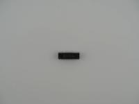
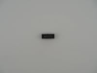
When I place this specific unit on the scale, the 2.7 gram reading immediately confirms the density of the ceramic package. This is not a cheap consumer plastic chip. Measuring just about 19mm across the ruler, this dense block of dark ceramic is a textbook example of late 70s and early 80s Cerdip packaging.
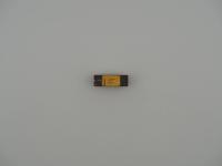
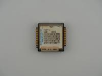
Here is the exact transcription of the surface text from the artifact:
Top Surface:MD2114AL-4/B
BL2262948
INTEL (m)(c) 1971
Bottom Surface:MALAY
DZ
226
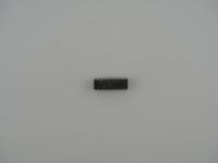
Holding this piece, the brutalist dark grey finish of the glass-sealed ceramic is striking. The matte texture feels chalky to the touch, a hallmark of military-spec thermal packaging. Looking closely at the 18 tin-plated pins, I can see they have a dull, oxidized patina. A few pins on the bottom row show slight outward bending. This tells me this chip was likely pulled from a high-retention socket rather than sitting New Old Stock in a tube for four decades. The Intel copyright stamp from 1971 is incredibly crisp, standing out in faint grey laser etching against the dark substrate.
Diving into the silicon itself, the 2114 is a 1024 word by 4-bit Static Random Access Memory (SRAM) chip. Fabricated using Intel's high-density NMOS technology, it does not require a clock or timing strobe, making it incredibly easy to integrate into early microcomputer buses.
This specific part number, MD2114AL-4/B, tells a serious engineering story. The "A" signifies an Advanced silicon revision over the original 1977 release, offering better margins and reliability. The "L" stands for Low Power. While early NMOS chips ran notoriously hot, this low power variant reduced current draw, a critical factor for densely packed memory boards. The "-4" suffix denotes an access time of 200 nanoseconds. By early 80s standards, 200ns was incredibly snappy for main system memory.
The real magic here is the "M" prefix and the "/B" suffix. This indicates Military specification. It is built to operate perfectly between brutal temperature extremes of -55 to +125 degrees Celsius. The "/B" confirms it was processed to MIL-STD-883 Class B standards, meaning it survived punishing environmental stress screening and rigorous electrical burn-in testing before leaving the fabrication plant.
The 2114 architecture is fundamentally the duct tape of the vintage computing era. If you crack open a Commodore VIC-20, investigate the motherboard of an Osborne 1, or inspect early arcade cabinets like Pac-Man and Donkey Kong, you will find banks of 2114 chips managing video RAM and system memory. They were ubiquitous, cheap, and reliable.
However, a very common misconception in the vintage hardware community revolves around the date. Novice collectors see the bold 1971 stamped right on the front and assume they have uncovered a remarkably early piece of silicon history. I always have to correct this. That date is simply the copyright year for the Intel logo itself. The 2114 architecture did not even exist until roughly 1977.
What makes this particular artifact special is its military pedigree. While standard commercial 2114s powered home video games, this ruggedized unit was destined for something much heavier. Chips with these MIL-STD ratings ended up in aerospace navigation boxes, defense tracking radar systems, and extreme industrial control mainframes.
I am highly confident in dating this specific artifact to the middle of 1982. When examining the bottom of the chip, we see the fab origin MALAY (Malaysia) next to a 226 stamp. Cross-referencing this with the top side lot code BL2262948, the "226" pattern emerges clearly. In the standard Intel date coding format of the era, "22" represents the year 1982, and "26" represents the 26th week of that year.
It is fascinating to see an American military-grade chip assembled in the Malaysian facilities during the early 1980s. During this era, Intel was aggressively expanding its offshore assembly and testing capabilities to keep up with massive global demand. Despite being assembled overseas, the strict MIL-STD-883 Class B testing means this chip was subjected to the exact same punishing QA protocol as a unit built in Santa Clara. It is a fantastic, heavy-duty example of the unsung SRAM workhorses that built the foundation of the digital revolution.