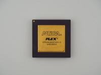
A mechanical jewelry. This artifact is a prime example of high-reliability packaging where cost was clearly not the primary concern.
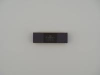
The chip is still suspended in its original non-conductive carrier ring. These delicate, gold-plated leads stretch outward like a suspension bridge from the ceramic body to the outer frame. When looking at the back of this board, you can see the protective dark plastic or ceramic bars clamped over the leads to prevent them from bending before the chip is finally excised and soldered onto a PCB.
The laser etching on the gold cap is highly legible and provides a wealth of identification data. Here is the exact surface text transcription:
AMCC 0313
Q20025-0091B
94117SOCN
315055P2
3/1350Z
[Delta Logo] U.S.A.
The ceramic body has a subtle, matte texture that contrasts sharply with the highly reflective gold lid and the brilliant sheen of the finely pitched pins. A very faint "R" is stamped into the bottom right corner of the rear ceramic face. The condition is pristine with zero bent pins, which is exactly why that carrier frame is there.
This artifact utilizes a CQFP (Ceramic Quad Flat Pack) package. This specific design is engineered for extreme environments. Ceramic does not absorb moisture like plastic packages do, which prevents "popcorning" or microscopic cracking when subjected to rapid thermal changes or vacuum environments. The massive gold lid is not just for show. It acts as an integrated heat spreader to pull thermal energy away from the silicon die inside.
The delicate lead frame is a masterclass in precision manufacturing. Because this chip has a high pin count, the leads are incredibly thin and closely spaced. If a manufacturer tried to ship this chip loose, the pins would be crushed instantly. The outer carrier ring allows automated testing equipment to interface with the chip and verify its functionality without ever touching or stressing the final solder joints. Right before installation, a specialized tool stamps the chip out of this frame and forms the leads downward into a gull-wing shape for surface mounting.
AMCC was highly regarded for building high-speed logic, bipolar, and BiCMOS gate arrays. Given the massive thermal footprint and the aerospace-grade packaging, it is highly likely the silicon inside is running a high-speed, power-hungry logic matrix designed for telecommunications routing or military signal processing.
Applied Micro Circuits Corporation (AMCC) is a name that commands respect among network engineers and telecom graybeards. While they never had the consumer household recognition of Intel or AMD, AMCC was the company you called when you needed to push massive amounts of data across fiber optic backbones.
In the late 1990s and early 2000s, AMCC was fabricating some of the most complex ASICs (Application-Specific Integrated Circuits) on the planet. They eventually pivoted into ARM server processors with their X-Gene architecture before being absorbed into MACOM.
Chips like this Q20025 represent the unsung heroes of the internet backbone and military infrastructure. They do not run operating systems or calculate 3D graphics. They sit in the dark inside a telecom switch or an avionics bay, routing gigabits of data with zero tolerance for failure. The myth of these chips is that they are "dumb" logic. In reality, routing that much data in hardware without bottlenecking requires brilliant architectural design.
Researching specific ASICs is always a thrilling challenge because these chips were never advertised to the public. They were sold directly to enterprise or military contractors in lots of thousands.
Based on the surface markings, I can confidently decode several key aspects of this artifact. The 0313 stamped next to the AMCC logo is almost certainly a date code indicating the chip was packaged in the 13th week of the year 2003. This aligns perfectly with the era when high-reliability ceramic packaging was still heavily utilized for specialized logic arrays before BGA (Ball Grid Array) completely took over the industry.
The primary part number Q20025-0091B strongly suggests this is part of a Q-series logic array. AMCC had a long history of Q-prefix gate arrays dating back to the 1980s. The 0091B suffix likely denotes the specific custom mask or logic configuration flashed onto the base gate array for a specific customer.
The U.S.A. stamp and the small delta logo confirm its domestic fabrication, which further reinforces the theory that this could be a military, aerospace, or critical infrastructure component. The lack of standard CPU architecture markings confirms we are looking at a highly specialized piece of custom silicon.