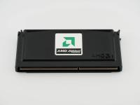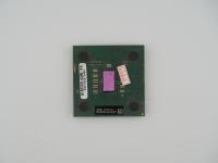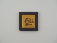
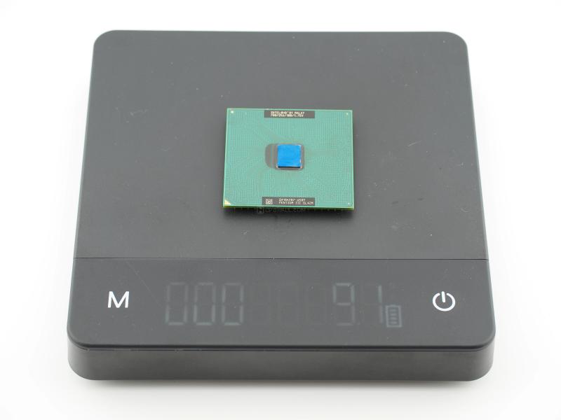
Holding this piece in the studio, the first thing that catches the eye is the beautiful, iridescent blue of the exposed silicon die sitting dead center on the green organic substrate. Weighing in at exactly 9.1 grams, this is a quintessential turn-of-the-millennium processor. It lacks the massive, heavy gold heat spreaders of the earlier Pentium Pro era or the ceramic heft of a classic Pentium, replacing them with a lightweight, cost-effective package designed for mass consumer adoption.
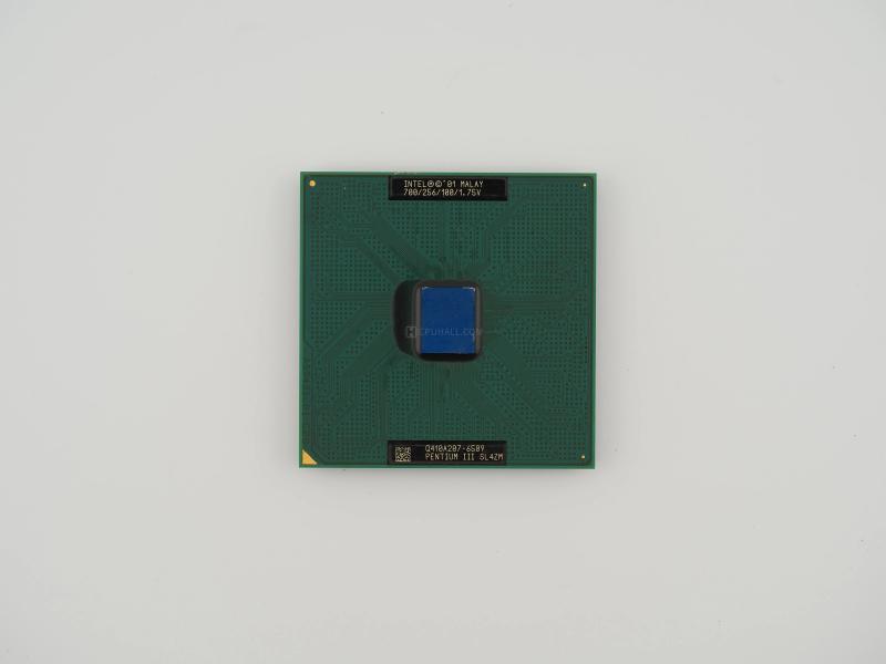
Examining the laser-etched text directly on the silicon die, the high-contrast markings are perfectly legible against the blue coating. I can clearly read the following factory specifications:
INTEL (m)(c) '01 MALAY
700/256/100/1.75V
Q410A207-6589
PENTIUM III SL4ZM
Down the left edge of the green substrate, a fainter factory code reads A59431 01 C28. The black epoxy underfill bleeding out slightly from under the silicon is completely intact, showing no signs of thermal degradation.
Flipping this artifact over reveals the staggered gold-plated pins characteristic of the Socket 370 interface. The center of the pin grid is populated by tiny Surface Mount Device (SMD) capacitors. Interestingly, a previous vendor slapped a paper warranty sticker directly over these delicate capacitors. The sticker bears the letters "LL & PJ" alongside the Chinese characters "撕毁无效" (Void if torn) and blank fields for the year, month, and day. It is a fantastic little detail that gives this specific unit a distinct grey-market or local-builder flavor.
This chip represents a massive structural shift in how Intel approached thermal management and packaging. Built on the 180nm fabrication node, this is the legendary Coppermine core. It packs 28.1 million transistors into a tiny die.
The most important engineering shift here is the FC-PGA (Flip-Chip Pin Grid Array) form factor. Intel had spent the previous few years putting processors onto large PCBs inside bulky plastic cartridges known as Slot 1. That was done because L2 cache chips were separate entities from the main processor die and needed to sit next to the CPU. With Coppermine, Intel finally managed to integrate the 256KB of L2 cache directly onto the processor die itself. They called this the Advanced Transfer Cache, and because it was on-die, it ran at the full 700 MHz core speed rather than a fraction of it.
Because the cache was now integrated, the massive Slot 1 cartridge was obsolete. Intel "flipped" the chip so the silicon die faced completely outward. This allowed the user's heatsink to make direct physical contact with the silicon, providing vastly superior thermal transfer compared to the older plastic-encased models. The core voltage requires a steady 1.75V, and the Front Side Bus (FSB) runs at an even 100 MHz, making it highly compatible with the ubiquitous 440BX chipset motherboards of the era.
The history of the exposed-die Pentium III is written in cracked silicon and the tears of PC builders. While the FC-PGA design was brilliant for thermal efficiency, it introduced a terrifying new risk. The naked silicon die is incredibly brittle.
During the late 90s and early 2000s, aftermarket heatsinks were heavy chunks of copper and aluminum held down by brutally stiff steel retention clips. The crunch. That was the sound every hardware enthusiast dreaded. If you angled the heatsink slightly wrong while pushing down on the socket clip with a flathead screwdriver, the edge of the heatsink would bite into the corner of the blue silicon die and chip a piece off. Countless Pentium III and AMD Athlon chips met a premature death this way. Looking at this specific unit under the macro lens, all four corners of the die are pristine. It survived the heatsink gauntlet.
This era was also the height of the Megahertz Wars. Intel was in a fierce, high-stakes battle with AMD to reach the 1 GHz mark first. While this 700 MHz model was not the flagship, it was the bread and butter of serious gaming rigs and power-user workstations, successfully fending off AMD's K6-2 and holding the line against the formidable early Athlon processors.
There is absolutely no mystery regarding the identity of this processor. The S-Spec number SL4ZM acts as a perfect fingerprint. Cross-referencing this code with Intel's historical documentation immediately confirms the exact specifications physically printed on the die.
The 700/256/100/1.75V string perfectly maps out the hardware capabilities. The 700 denotes the 700 MHz clock speed, 256 is the 256KB of L2 cache, 100 is the 100 MHz FSB, and 1.75V is the VCore requirement. The copyright year of 2001 etched on the die is slightly later than the initial 1999 launch of the Coppermine architecture, indicating this specific piece was likely fabricated toward the tail end of the Pentium III's mainstream lifecycle before the Pentium 4 completely dominated Intel's production lines.
The inclusion of the Chinese warranty sticker on the underside suggests this unit lived a long, practical life in the Asian secondary market before finding a permanent home in the archives. It is a perfect, unblemished example of one of the most consequential consumer architectures Intel ever produced.