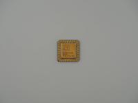
While a lot of the pieces in my collection focus on the raw, exposed ceramic and pristine gold of mainframe modules, there is a distinct, heavy-metal charm to this sealed black plastic cartridge. The front face features a stylized, embossed AMD logo set into the matte black plastic, flanking a pristine metallic foil sticker that proudly announces the brand.
Flipping it over reveals a massive black anodized aluminum backplate with mounting holes designed to dissipate heat from the thermal plate resting against the die inside. At the bottom, peering out from the plastic housing, is the gold edge connector.
Here is the exact transcription of the surface markings found across the top spine and bottom edge:
Top Spine Etching:
AMD-K7500MTR51B C
219939029464
Top Edge Print:
AMD ATHLON™ PROCESSOR
Bottom Edge Print:
(m) (c) 1999 AMD
Assembled in the USA
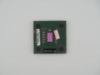
Let us get into the weeds of the hardware hiding under that plastic shroud. This specific unit represents a radical shift in desktop packaging driven entirely by thermal and cache limitations of the era. The die itself is based on the K7 "Argon" core, manufactured on a 250nm process. Because on-die L2 cache was too difficult and expensive to yield at high capacities in 1999, AMD had to mount separate SRAM chips right next to the processor die on a single PCB. To protect this multi-chip layout and provide a massive surface area for cooling, they enclosed the whole thing in this Single Edge Contact Cartridge (SECC).
The most brilliant engineering move here was the bus architecture. AMD licensed the EV6 front-side bus protocol directly from DEC, the creators of the legendary Alpha architecture. This allowed the Athlon to communicate with the motherboard at an effective 200 MHz, leaving Intel's 100 MHz and 133 MHz front-side buses in the dust. The 51B in the part number is a critical technical identifier. It dictates that the 512KB of off-die L2 cache runs at exactly one-half of the core clockspeed, which was a necessary compromise to maintain stability using external SRAM chips at 500 MHz.
This chip is the exact moment AMD stopped playing catch-up and started throwing absolute haymakers. For years, AMD was viewed as a budget alternative to Intel. The K7 architecture changed everything. It was faster, it was aggressive, and it set the stage for the legendary race to the 1 GHz milestone.
The most notorious piece of hardware lore surrounding this artifact is the "battle of the slots." If you look at the edge connector, it is physically identical to Intel's Slot 1 interface. AMD did this intentionally to allow motherboard manufacturers to use the exact same physical slot hardware on their assembly lines. However, the pinout and electrical signaling were completely different. A common myth was that you could run an Intel chip on an AMD board. In reality, plugging an Athlon into an Intel motherboard, or vice versa, would result in absolute failure and a potential cloud of magic smoke.
Furthermore, this specific cartridge style birthed the era of the "Goldfinger" devices. Extreme overclockers realized that if you violently cracked open this plastic shell, you could find a small proprietary connector on the top edge of the PCB. By attaching a custom aftermarket circuit board to these contacts, you could manually override the processor's multiplier and voltage, pushing these 500 MHz chips to absurd limits.
The visual evidence on this piece leaves absolutely zero room for doubt. The part number AMD-K7500MTR51B is a standard AMD Ordering Part Number (OPN). Breaking down the nomenclature confirms every aspect of the chip. "K7" denotes the architecture. "500" confirms the operating frequency of 500 MHz. "M" specifies the SECC cartridge package type. "T" indicates the standard 1.60V core voltage for this stepping. Finally, "51B" confirms the 512KB L2 cache operating at a 1/2 fractional speed of the core clock.
The bottom markings stating (m) (c) 1999 AMD align perfectly with the original launch window of the Argon core in mid-to-late 1999. The "Assembled in the USA" stamp further authenticates the origins of the final cartridge packaging before AMD shifted the majority of their assembly completely offshore. It is a textbook, pristine example of the genesis of the Athlon dynasty.