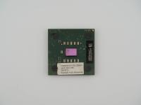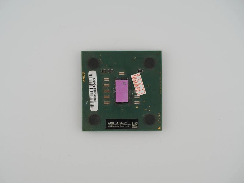
We have moved away from the heavy, exotic ceramics of mainframe hardware into the era of the Organic Pin Grid Array. The green fiberglass substrate is standard, but the aesthetic is defined entirely by the exposed silicon die resting dead center. The die has a distinct purplish hue and a mirror finish that catches the light perfectly.
Looking closely at the PCB surface, we can see surface mount capacitors bridging the traces around the central die. The right edge clearly reads ASSEMBLED IN MALAYSIA in gold lettering alongside a small batch number 27493.
The most prominent feature is the black laser etched identification label located at the bottom edge:
AMD Athlon™
AXDA2600DKV4D T841566B40960
AQYHA 0406VPMW (M)(C) 1999 AMD
There is some visible wear and accumulated dust on the four black foam spacer pads. These pads were essential structural components designed to keep aftermarket coolers leveled. Interestingly, this artifact still bears a white paper barcode sticker (500102567046S) and a Chinese vendor warranty seal reading "兆霖科技" (Zhaolin Technology) with a blank date field.
This specific unit utilizes the celebrated Barton core. Built on a 130 nanometer copper interconnect fabrication node, Barton represented the absolute peak of the K7 microarchitecture.
The engineering philosophy here favored pure instructions per clock over raw frequency. AMD achieved this by doubling the L2 cache from 256KB on the previous Thoroughbred core up to a massive 512KB for Barton. This massive cache injection required a larger die size, utilizing approximately 54.3 million transistors.
Thermally, this chip was a brute force instrument. Operating at a default voltage of 1.65V, it generated significant heat in a very concentrated footprint. The lack of an Integrated Heat Spreader meant the bare silicon made direct contact with the heatsink base. While this provided superior thermal transfer theoretically, it created a massive mechanical point of failure.
The history of the Athlon XP is the history of AMD putting Intel against the ropes. Intel was pushing the NetBurst architecture, chasing high gigahertz numbers at the expense of efficiency. AMD countered with the "Performance Rating" system. This chip only clocks at 1.917 GHz, but the 2600+ moniker explicitly told consumers that it would match or beat a 2.6 GHz Pentium 4 in real world tasks. It was a bold marketing strategy that actually held up in benchmarks.
The lore surrounding the Socket A era is almost entirely dominated by tales of crushed silicon. PC builders in the early 2000s had to mount heavy, solid copper heatsinks directly onto that fragile, exposed purple die. A single slip of a flathead screwdriver on the incredibly stiff socket retention clips would crack the edge of the die, instantly killing the processor. Seeing an intact die on a heavily used chip like this is always a relief.
The black identification label gives us absolute certainty regarding the provenance and technical specifications of this exact artifact. The OPN strings are a treasure trove of data for hardware archivists.
Breaking down AXDA2600DKV4D:
The stepping code AQYHA and the date code 0406 are where things get highly specific. The 0406 signifies that this chip rolled off the assembly line in week 06 of the year 2004. This is a critical detail. In late 2003, specifically around week 39, AMD initiated "Super Locking" to combat unscrupulous vendors who were remarking cheaper CPUs as higher tier models. Because this unit was manufactured in 2004, we can state with near absolute certainty that the clock multiplier is hard locked internally, preventing the easy front side bus overclocking that made earlier stepping Barton cores legendary among enthusiasts.