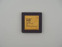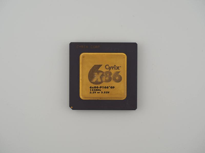

The high-contrast aesthetic of the late 90s CPU wars is perfectly encapsulated right here. The top features a dark, dense ceramic substrate dominated by a massive, glorious gold-plated heat spreader.
The micro-contrast on the macro shots reveals the exact surface text etched into the materials.
Front text transcription:
CYRIX CORP
Cyrix 6x86
6x86-P166+GP
133MHz
3.3V or 3.52V
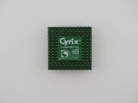
Flipping the board over reveals the intricate brazing of the 296 gold pins and four surface-mounted capacitors surrounding the central silicon encapsulation. The macro lens perfectly caught the faint, low-contrast laser etching on this underside material.
Rear text transcription:
COPYRIGHT USA
1995 CYRIX
[Faint alphanumeric batch code]
MADE IN
CANADA
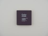
The gold cap has a few micro-scratches indicative of a previously mounted heatsink, but the pins are impeccably straight and the ceramic corners are sharp and unchipped. It is a brilliant display piece.
Underneath that gorgeous gold cap lies the "M1" core. Cyrix was a fabless semiconductor company, meaning they designed the brains but lacked the multi-billion dollar factories required to actually print the silicon. For the 6x86, they partnered heavily with IBM to manufacture the chips.
The architecture here is remarkably aggressive for its era. The M1 core featured super-scalar execution and out-of-order execution capabilities well before Intel implemented them in the standard Pentium line. The engineering goal was pure instruction throughput per clock cycle.
However, this chip ran exceptionally hot. The massive gold-plated cap wasn't just for looking incredibly cool. It was a functional necessity to draw heat away from the die. The power draw and thermal output were notoriously difficult to manage with the standard aluminum heatsinks of the mid-1990s. The markings clearly state a voltage of "3.3V or 3.52V". This flexibility was required because early Socket 7 motherboards had varying voltage regulator designs, and running this chip at the higher 3.52V practically demanded a massive cooling fan to prevent systemic lockups.
This specific artifact represents one of the most brilliant and controversial marketing moves in computing history. Notice how the chip operates at a physical clockspeed of 133 MHz, but it is boldly branded as a P166+.
Cyrix essentially invented the "Performance Rating" (PR) system. Their out-of-order architecture was so efficient at standard integer mathematics that a 133 MHz Cyrix chip could easily trade blows with, or outright beat, a 166 MHz Intel Pentium in standard Windows applications. Cyrix decided the clock speed metric was unfair and began naming their processors based on their performance equivalence to Intel's flagship parts.
The lore surrounding this chip is legendary among retro enthusiasts. It was the ultimate underdog darling for budget system builders. You could buy this chip for a fraction of the cost of a true Pentium 166 and get incredible office and 2D performance.
But there was a fatal flaw. The floating-point unit (FPU) on the 6x86 was decidedly weak. When ID Software released Quake, which relied heavily on complex floating-point math to render its 3D environment, the Cyrix 6x86 completely choked. Gamers quickly realized that while the PR rating was honest for spreadsheets, it was a total illusion for 3D gaming. This single software release arguably sealed the fate of the 6x86 in the consumer enthusiast space.
The visual clues on this exact unit provide a perfect map of its origin story. Cyrix relied on two main foundries to produce the 6x86 line. One was SGS-Thomson, and the other was IBM.
Looking at the high-fidelity macro shot of the underside, the MADE IN CANADA etching is the definitive smoking gun. IBM operated a massive semiconductor packaging facility in Bromont, Quebec. The silicon wafer itself was likely printed at an IBM fab in the United States or Europe, but it was shipped to Bromont where it was sliced, wired, and sealed into this specific ceramic and gold package.
The GP suffix on the front face denotes a standard ceramic package, differentiating it from later, cooler-running split-voltage variants. The definitive link between the 1995 copyright date and the IBM Canada packaging facility cements this as a true mid-90s heavyweight from the height of the alternative x86 clone wars.