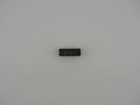
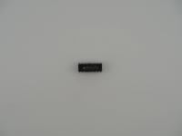
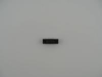
The ignition key to the digital revolution. It is a tiny but impossibly dense block of computing history. The packaging is a glorious CERDIP (Ceramic Dual In-line Package) featuring a dark charcoal-grey ceramic body.
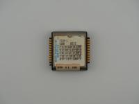
Manufacturer Logo: Vintage Intel "dropped-i"
Part Number: C8008-1
Batch Code: H3953
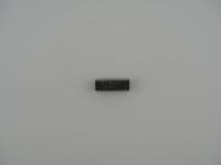
The physical textures are stunning. The top is dominated by a heavy gold-plated cap that reflects light beautifully, showing just a hint of vintage patina. The black ink stamping is remarkably crisp, featuring the classic early-70s Intel logo with the disconnected square dot over the "i". The side-brazed pins are thickly plated in gold. Looking closely at the side profile and bottom, the ceramic is completely blank and smooth, emphasizing the raw, functional design of early silicon packaging. It is a heavy metal piece of engineering art.
Diving into the technical weeds reveals a chip defined by intense compromise. The original 8008 was built on a 10-micrometer PMOS (p-channel metal-oxide-semiconductor) process and contained roughly 3,500 transistors. This specific piece is the C8008-1. The "-1" suffix is absolutely critical. It denotes a highly binned, faster speed grade. While the standard 8008 plodded along at 500 kHz, this high-performance variant was rated for a blistering 800 kHz.
The most fascinating engineering bottleneck of the 8008 is its physical package. Intel forced this architecture into an 18-pin form factor simply because they already owned high-volume manufacturing tooling for 18-pin memory chips. This severe pin limitation meant the chip could not have separate pins for its 14-bit address bus and 8-bit data bus. The CPU had to multiplex everything. It pushed data and addresses out in a complex, multi-state phase sequence. If you wanted to build a computer around this chip, you needed dozens of external TTL logic chips just to decode the signals and talk to memory. It was an absolute nightmare to implement on a motherboard, but the raw capability it provided was unprecedented.
The history of the 8008 is a story of rejection and accidental triumph. The chip was originally commissioned by the Computer Terminal Corporation (CTC) to power their Datapoint 2200 programmable terminal. CTC gave Intel the instruction set and asked them to put it on a single chip. However, Intel struggled to meet the performance requirements and the deadline. CTC eventually rejected the silicon outright, choosing instead to build their terminal using a massive board full of standard TTL logic gates.
Left with a finished chip and no primary buyer, Intel decided to market the 8008 to the general public. It changed the world. This chip became the beating heart of the very first commercial microcomputers, most notably the French Micral N and the American SCELBI-8H. It proved that a general-purpose computer could exist on a desktop.
A common myth is that the 8080 was a completely new design from scratch. In reality, the 8008 is the direct grandfather of the 8080, which in turn spawned the 8086, which spawned the x86 architecture that likely powers the machine you are using to read this right now. Every modern Intel Core processor owes its lineage to the instruction set baked into this 1.8-gram block of ceramic.
The visual evidence on this artifact is definitive and completely aligns with Intel's early fabrication practices. The "C" prefix in C8008-1 explicitly designates the side-brazed ceramic package. Intel reserved these packages for higher-end applications and severe temperature tolerances, whereas consumer-grade chips typically received the cheaper plastic "P" or standard ceramic "D" packaging later on.
The H3953 marking is a classic Intel lot trace code from the era before they fully standardized their YYWW (Year-Week) date stamping conventions. The presence of the blocky "dropped-i" logo solidifies its early 1970s origin, as Intel transitioned to a more modern logo styling later in the decade. Finding a binned 800-kHz part in this pristine, side-brazed configuration is incredibly rare. The pins are straight and the brazing points show no signs of board extraction stress, suggesting this piece may have spent its life as a preserved spare or an unused engineering sample. It is a museum-grade specimen.