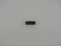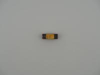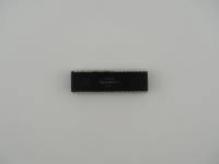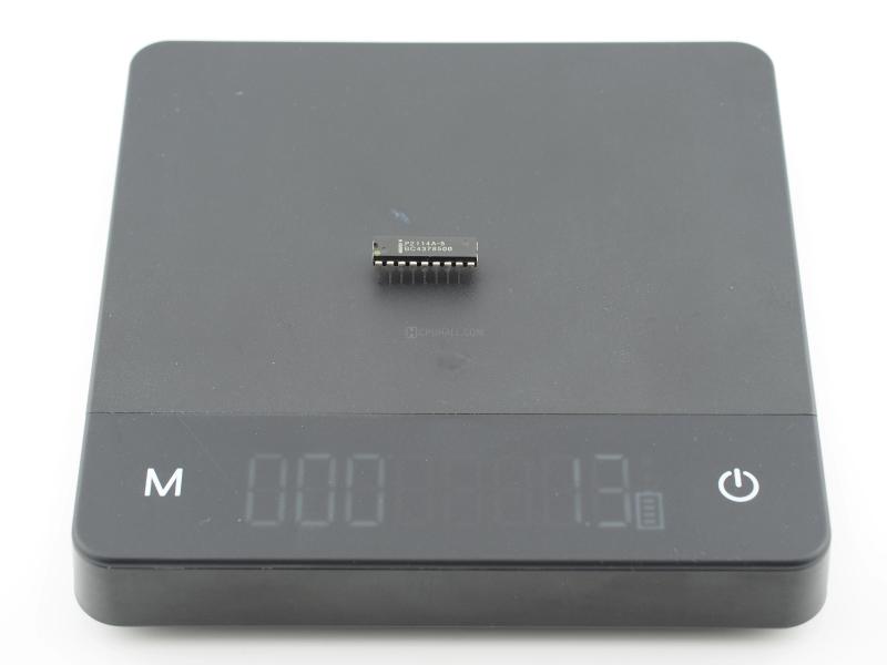
Holding this artifact in my hand, it feels like the pure utilitarian bedrock of the early computing era. Here we have a standard plastic Dual In-line Package memory chip. It is not made of gorgeous white ceramic, nor does it have brazed gold pins. It is a humble, functional block of black resin weighing exactly 1.3 grams and measuring roughly 23 millimeters across.
When observing the surface details under the light, the laser etching is remarkably clean for a mass-produced chip of its age.
Top Etching:i P2114A-5
BC4378500
Bottom Mold/Stamp:US 8429
BARBADOS
(A) 36
The lowercase 'i' immediately confirms its Intel pedigree. The bottom markings are just as interesting. The 8429 date code tells me this specific unit was baked in the 29th week of 1984, assembled in Barbados. Intel relied heavily on offshore facilities in places like Barbados, Malaysia, and the Philippines during this era to keep up with the staggering demand for microcomputer memory. The physical pins remain straight and practically untarnished, suggesting this chip was likely pulled carefully from a socket rather than destructively desoldered from a dead PCB.
The Intel 2114 is a 1024-word by 4-bit Static Random Access Memory (SRAM) chip. While 512 bytes sounds utterly microscopic today, in the late 1970s and early 1980s, it was a perfectly sized building block.
Because it is Static RAM, it does not require the complex external clocking and refresh logic that Dynamic RAM (DRAM) demands. You feed it power, give it an address, and it reliably holds the data. This simplicity made it the go-to memory for engineers who needed fast, uncomplicated storage buffers.
The 'A' in the P2114A part number denotes an architectural improvement over the original 1977 silicon. Intel moved these from their older NMOS process to their more efficient HMOS (High-performance N-channel MOS) technology. This shrink reduced power consumption and improved speed. The '-5' suffix indicates the speed bin, generally denoting a 250-nanosecond access time. It requires a standard 5V power supply and features identical power and ground pinouts to practically every other logic chip in its class, making PCB routing a breeze for hardware designers.
While mainframes had exotic core memory and early PCs wrestled with unstable DRAM banks, the 2114 SRAM quietly powered the entertainment revolution. If you have ever played a golden age arcade cabinet, you have relied on banks of these exact chips.
System architects used the 2114 extensively for video RAM, color RAM, and tilemap storage. Open up a Pac-Man, Galaga, or Donkey Kong arcade board, and you will see rows of 2114 chips. They were also the backbone of the Commodore VIC-20 home computer.
In the vintage hardware repair community, the 2114 has a notorious reputation. They ran notoriously warm and were prone to failure after decades of thermal cycling in poorly ventilated arcade cabinets. When a vintage game boots up with garbled sprites or a checkerboard of random colors, a dead 2114 is almost always the prime suspect. They are a repair technician's bread and butter. Finding a working, clean pull like this one is always a welcome sight on the workbench.
There is no mystery regarding the identity of this chip. The part number convention is one of the most thoroughly documented in computing history. The Intel databooks from the early 1980s perfectly match the physical characteristics, pin count, and nomenclature seen in the photographs. The "P" prefix simply denotes the plastic DIP package material, separating it from the more expensive "C" (ceramic) or "D" (cerdip) packages Intel offered for military or industrial applications.
This specific unit was undeniably destined for a consumer electronics device or an arcade motherboard. Given the 1984 date code, it rolled off the assembly line right as the 8-bit era was peaking, likely serving in a late-model home computer or a mid-80s coin-op machine.