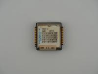
Holding this piece, the first thing that strikes you is the density. I tossed this specific unit onto the scale and it clocked in at a solid 8.7 grams. That weight comes from the thick, dark grey ceramic package holding the silicon.
The faint, slightly degraded white laser etching against the textured ceramic read:
Top Markings:D27512
K9114902
(m) (C) i '83
Bottom Markings:KOREA
8908
D2A11B
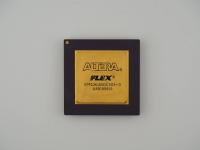
Right in the center is the defining feature of this chip: the round quartz window. Looking through that tiny porthole allows you to see the actual silicon die and the microscopic gold bonding wires bridging the gap to the lead frame. The pins themselves show a bit of oxidation and wear, typical for a component that was likely socketed and removed a few times during its operational life. Flipping it over reveals a completely different texture on the black underside, stamped plainly with its Korean assembly origin and an 8908 date code indicating it was put together in the 8th week of 1989.
This is a classic UV-erasable programmable read-only memory chip, or EPROM. The 27512 designation tells us exactly what we are dealing with mechanically. It holds 512 kilobits of data, organized as 64K words by 8 bits (64 KB total).
The engineering behind that quartz window is brilliant and entirely functional. The memory relies on floating-gate transistors. To write data to the chip, you apply a higher-than-normal programming voltage (usually around 12.5V for these later 27-series chips) to force electrons into the floating gate, altering the state of the cell. Because the gate is electrically isolated, those electrons stay trapped there indefinitely, holding your code.
To erase the chip and start over, you expose the bare silicon die to intense ultraviolet light (specifically UV-C) for about 20 to 30 minutes. The UV photons excite the trapped electrons enough to jump the oxide barrier, resetting the entire array to all ones. That is exactly why the expensive quartz window is necessary. Standard glass blocks UV light, so pure quartz had to be brazed into the ceramic lid to allow the erasure process.
If you opened up an arcade cabinet, a piece of industrial control equipment, or a desktop computer motherboard from the mid-1980s to the early 1990s, you would find a row of these EPROMs staring back at you. They were the standard for storing firmware and executable code before flash memory became cheap and ubiquitous.
The greatest lore surrounding these chips involves the "sticker of death." In a production environment, that beautiful quartz window was strictly a liability. Once programmed, it had to be covered with an opaque sticker, often metallic foil. A persistent hardware myth of the era was that a camera flash could erase the chip. While a single flash would not wipe it, leaving an uncovered EPROM under bright fluorescent office lights for a few weeks or near a sunny window absolutely could cause bit rot, flipping a few random bits and instantly bricking whatever machine it was installed in. Finding an old arcade board with missing EPROM stickers is a classic warning sign of impending hardware troubleshooting.
There is no mystery regarding the identification of this artifact. The evidence is carved right into its surface. The standard D27512 is the universal Intel part number format for a ceramic EPROM of this capacity. The lowercase "i" wedged next to the 1983 copyright date is the definitive Intel branding mark for their silicon IP of this era.
Interestingly, while the architecture and mask copyright date to 1983, the 8908 marking on the back indicates this specific chip was manufactured much later, in early 1989. This massive gap between copyright and assembly highlights just how long the production lifecycle was for these essential memory chips. They were fabricated continuously for years to feed the insatiable demand of the embedded electronics market.