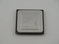
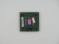
The reverse side of the package is a stark, matte slab of dark purple ceramic, bearing nothing but a simple MALAYSIA stamp indicating its assembly origin. But flipping this artifact over reveals the true spectacle. The top face is dominated by a massive, highly reflective gold-plated cap. The 68 gold-plated traces fan out from the center like a sunburst, wrapping around the edges of the ceramic package to form the leadless contacts.
You can clearly see the striking micro-contrast of the laser etching cut directly into that gold cap. The surface text reads exactly as follows:
[AMD Arrow Logo]
R80286-8/C2H
8630FP
(m) (C) INTEL 1982
The physical texture of the ceramic is pristine, showing very little wear. The gold cap has some microscopic surface scuffs visible under harsh lighting, but the brazing of the traces to the ceramic substrate is a masterclass in 1980s material engineering. The visual juxtaposition of the AMD logo directly above an Intel copyright stamp is the real star of the show here.
This silicon represents a massive leap forward from the 8086 era. The 80286 architecture packed roughly 134,000 transistors onto the die, fabricated using a 1.5-micron process. This specific unit operates at a conservative 8 MHz, which was standard for the mid-1980s AT clones, though AMD would eventually push their 286 chips to blistering speeds of 16 MHz and even 20 MHz, far outpacing Intel's own offerings.
The CLCC (Ceramic Leadless Chip Carrier) form factor used here was a robust, thermally efficient packaging choice. The solid ceramic substrate and the large metal cap worked together to dissipate heat, allowing the chip to run reliably without the need for active cooling. Architecturally, the 286 introduced "Protected Mode," expanding addressable memory to a theoretical 16 megabytes and adding hardware-level multitasking support. The implementation was famously clunky. Getting out of Protected Mode back into Real Mode required physically resetting the processor, a quirky design choice that gave systems programmers massive headaches.
This specific artifact is a physical manifestation of one of the most consequential legal and business relationships in computing history. When IBM was designing the original PC, they demanded a second source for the microprocessor to ensure supply chain stability. Intel was forced to license their precious x86 designs to competitors. AMD stepped up, signing a technology exchange agreement in 1982.
This chip is the direct result of that forced marriage. You are looking at a processor fabricated and marketed by Advanced Micro Devices, using a mask and microcode completely owned by Intel. It is a licensed clone. By the late 1980s, Intel realized they were creating their own worst enemy and famously refused to hand over the designs for the subsequent 80386 processor. That decision sparked a massive, bitter, decade-long legal war between the two giants. Seeing the AMD arrow logo sitting right next to (C) INTEL 1982 on the exact same piece of gold is a hilarious and historically rich paradox. It is the hardware equivalent of a peace treaty signed moments before a nuclear war.
I am completely confident in the identification and historical placement of this artifact. The laser-etched markings provide a perfect forensic timeline. The 8630 date code tells us this exact piece of silicon was finalized in the 30th week of 1986. The R prefix in the part number R80286 typically designates the specific ceramic LCC package type in AMD's internal cataloging system from that era.
The -8 confirms the 8 MHz binning. The C2H string likely relates to the specific stepping or fabrication batch. Finding these chips in the standard PGA (Pin Grid Array) format is quite common, but the CLCC variant seen here is visually superior and slightly harder to track down in pristine condition. It perfectly encapsulates the era of second-source manufacturing before the x86 market fragmented into fiercely proprietary architectures.