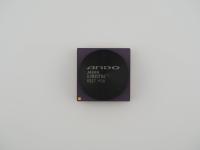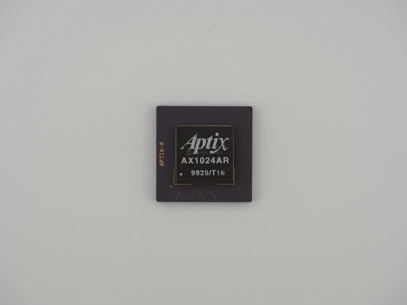

This is a massive piece of high-grade ceramic, built strictly for enterprise prototyping environments where cost was a secondary concern. The dark purple ceramic substrate feels incredibly substantial. Looking closely at the face of the artifact, the original fabricator marks and batch codes are clearly visible against the dark background.
Aptix
AX1024AR
9926/T16
APTIX-R (Printed vertically on the left margin)
The date code 9926 tells me this piece was packaged in the 26th week of 1999. The central metallic cap is secured with a highly visible, thick gold braze that catches the light beautifully. There is also a fascinating human element to this specific chip: the numbers 2.35 are handwritten in a faint marker directly onto the bottom edge of the ceramic. This is almost certainly an engineer's marking, perhaps indicating a specific voltage requirement, a firmware revision, or a routing timing threshold used during a prototyping run.
Flipping the chip over reveals a stunning, immaculate grid of gold-plated pins. The Pin Grid Array is dense and uniform, save for four intentional indexing gaps near the center of the matrix. The physical condition is pristine, with no bent pins or thermal discoloration, suggesting it was carefully extracted from its prototyping board.
This artifact is not a central processing unit in the traditional sense. It has no instruction set architecture and executes no code. Instead, the Aptix AX1024AR is a Field Programmable Interconnect Device (FPID).
In the late 1990s, if a company wanted to design a complex new processor or ASIC, they could not just send the untested design to a fabrication plant. They had to test it first. Engineers would map their unreleased chip designs across dozens of separate FPGAs. The problem was getting all those individual FPGAs to talk to each other with the correct timing and signal integrity.
That is exactly where this Aptix chip came in. It acted as a massive, ultra-fast programmable switchboard. The "1024" in the part number very likely refers to the massive number of programmable I/O routing channels it could handle simultaneously. Engineers would slot several of these into an Aptix System Explorer board, and the AX1024AR would dynamically route thousands of electrical signals between the various FPGAs. It is essentially a piece of raw networking silicon for other silicon. The massive CPGA form factor was entirely necessary simply to break out that extreme number of physical signal paths to the motherboard.
The engineering behind this chip is fascinating, but the history of the Aptix Corporation is absolute insanity.
Aptix was founded by Amr Mohsen, a brilliant engineer who held numerous patents in semiconductor design. The company built a very solid business selling prototyping systems utilizing chips exactly like the one we have here. But in the early 2000s, Mohsen sued EDA giant Mentor Graphics, claiming they infringed on an Aptix patent.
During the trial, Mentor Graphics discovered that Mohsen's critical evidence (a personal engineering notebook detailing his early inventions) was entirely fabricated. Mohsen had artificially aged the notebook and forged entries to pre-date Mentor's work. When Mohsen realized he was going to be caught, he attempted to flee the country but was arrested by the FBI with a passport and a bag of cash.
It gets worse. While sitting in federal custody awaiting trial for perjury, Mohsen approached a fellow inmate and attempted to hire a hitman to assassinate the federal judge presiding over his case. The inmate informed the FBI, who recorded the entire plot. Mohsen was ultimately sentenced to 24 years in federal prison. Aptix, completely drained of funds and leadership, spiraled into bankruptcy. This piece of silicon represents the height of the company's engineering prowess, right before it was destroyed by one of the most spectacular executive meltdowns in tech history.
Identifying this artifact required moving away from standard CPU archives and digging into historical Electronic Design Automation literature.
The Aptix stylized logo immediately points away from consumer hardware. The major clue here is the form factor combined with the 1999 date code. During this era, Aptix was aggressively marketing their System Explorer prototyping boards, which utilized massive proprietary routing matrices. Cross-referencing the AX1024AR part number with archived EE Times articles and vintage EDA datasheets confirms its identity as a Field Programmable Interconnect Device.
While exact datasheets for the AX1024AR are locked away in dead corporate archives, the technical lineage is clear. The handwritten 2.35 marking strongly implies this specific unit was an active participant in a hardware testbed. It is a brilliant, heavy, and historically loaded piece of engineering that perfectly bridges the gap between raw hardware capabilities and Silicon Valley hubris.