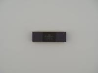
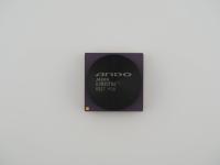
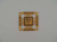
Clocking in at exactly 57.5 grams on the scale, this specific unit is an absolute brick of early-2000s supercomputing silicon. It features a stunningly thick, matte-finish metal heat spreader perfectly bonded to a dense white ceramic substrate.
When inspecting the laser-etched surface text under the light, the micro-contrast reveals the following markings:
XDRIDGE 1.1
SGI ©® 1999
099-0182-002
06K0906
0109
B08014F7
PQ ®©M
0109 B08014F7 099-0182-002 IBM
The presence of both the SGI logo and the classic 8-bar IBM logo on the bottom edge confirms a fabrication partnership. Flipping the chip over reveals a breathtakingly dense CPGA (Ceramic Pin Grid Array). Estimating the grid, there are well over a thousand individual pins packed tightly into the ceramic base. I can clearly see a cluster of bent and mangled pins along one of the outer edges, suggesting this chip was aggressively pulled from its socket or took a rough tumble in a scrap bin at some point in its life.
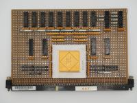
To understand what this chip does, you have to look at the massive modular architecture of SGI supercomputers from this era. This is a routing and interface ASIC. Specifically, it is the bridge chip that sat between SGI's proprietary high-speed XIO interconnects and standard PCI-X buses.
In systems like the Origin 3000 and the Onyx 3000, the main memory and processors were tied together using a hub ASIC called Bedrock. To get data out to storage arrays, networking cards, or InfiniteReality graphics pipelines, the data had to travel over XIO links. This ASIC handled that translation. The XIO links operated at 400 MHz over 16-bit differential connections, pushing a massive 800 MB/s of bandwidth in each direction for a combined 1.6 GB/s throughput per port.
Fabricated by IBM Microelectronics, likely on a 0.25-micron or 0.18-micron CMOS process, the logic gates required to buffer and translate these high-speed packets generated severe thermal loads. That completely explains the thick, brazed-on metal cap. The massive pin density of the CPGA package was an absolute necessity for routing multiple wide, high-frequency bus channels directly into the motherboard without creating signal crosstalk.
SGI's ccNUMA (Cache-Coherent Non-Uniform Memory Access) systems were legends of the visual computing and scientific world, scaling up to 512 MIPS processors and terabytes of RAM. But the absolute best part of this specific piece of history is right there on the top line of the laser etching: XDRIDGE 1.1.
SGI never released an "Xdridge" chip. The architecture manuals strictly refer to this component as the Xbridge ASIC. You can imagine the scenario: SGI engineers design a multi-million dollar supercomputer interconnect fabric, send their Verilog and masks off to IBM for fabrication, and the early batch of silicon comes back permanently branded with a hilarious typo. It is an amazing piece of physical hardware humor.
The Xbridge itself was the unsung hero of SGI's later years. By bridging proprietary supercomputer interconnects to standard PCI buses, it allowed SGI to utilize off-the-shelf storage and networking hardware, saving them from having to invent proprietary XIO expansion cards for every single enterprise use case.
I am completely confident in this identification despite the typo on the heat spreader. While the surface clearly reads "XDRIDGE", an exhaustive search through SGI's technical manuals for the Origin 300, Origin 3000, and Fuel workstations exclusively details the "Xbridge" ASIC acting as the interface between the system's Bedrock routing chip and the PCI expansion slots.
Furthermore, the part number 099-0182-002 perfectly aligns with SGI's internal nine-digit alphanumeric numbering scheme for components and logic boards. The 1999 copyright date printed on the silicon matches the late 1999 to early 2000 rollout and architectural finalization of the SGI SN1 architecture (which powered the Origin 3000 series). The IBM fab mark confirms the established historical relationship between the two companies, as IBM Microelectronics served as the primary foundry for many of SGI's custom routing ASICs during the NUMAflex era.