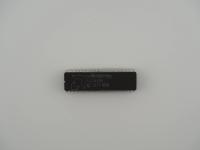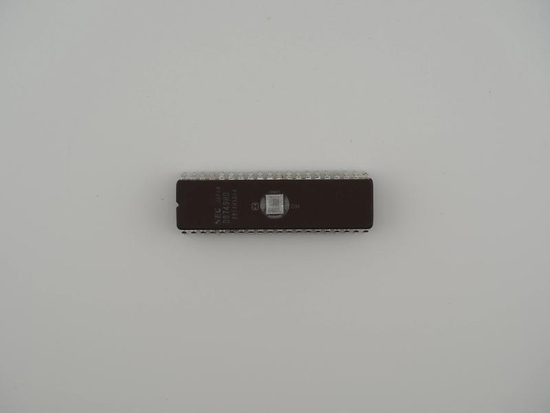

Weighing in at exactly 11.4 grams, this artifact is a heavy, gorgeous slab of late 1980s engineering. The package is a classic 40-pin Ceramic Dual In-line Package (CDIP-40), featuring a very dark, almost chocolate-brown ceramic substrate.
Looking closely at the side profile, you can see the thick white glass frit seal sandwiching the upper and lower ceramic halves. The pins themselves show a completely natural level of oxidation and wear for their age, with the tin or silver plating losing some of its factory luster.
The markings are crisp and fully legible under standard lighting:
NEC JAPAN
D8749HD
8811HX014
The absolute star of the show here is the circular quartz window right in the center of the package. When I put this under my 45mm macro lens, the window provides a crystal-clear view into the heart of the chip. You can easily make out the square silicon die and the incredibly fine wire bonds connecting the die to the external lead frame. The window is pristine, completely free of the cloudy degradation or scratches you sometimes see on heavily used erasable programmable read-only memory (EPROM) windows. It is currently resting in my 125L dry cabinet, locked at a stable 40% relative humidity, to ensure the metal contacts and internal bonding wires remain exactly as they are.
The NEC D8749HD is a direct second-source clone of the legendary Intel 8749 microcontroller, which belongs to the famous MCS-48 architecture family. This is an 8-bit microcontroller built on N-channel metal-oxide-semiconductor (NMOS) technology.
What makes the 8749 specific is its memory configuration. It contains 2 kilobytes of EPROM right there on the die, alongside 128 bytes of random-access memory (RAM). The quartz window exists for one specific purpose: erasure. By exposing the silicon die to strong ultraviolet (UV-C) light for about 20 to 30 minutes, the trapped electrons on the floating gates of the memory cells are energized enough to escape. This resets the memory back to its default state, allowing engineers to reprogram the chip with high voltage (typically around 21 volts) over and over again during development.
The chip operates on a standard 5V logic level and provides 27 input/output lines, making it incredibly versatile for controlling hardware peripherals. The 11 MHz maximum clock speed might sound crawling by today's standards, but in the realm of 1980s embedded control, it was more than enough muscle to drive complex mechanical and digital systems.
The Intel MCS-48 family was a monumental milestone in silicon history. Introduced in the late 1970s, it was essentially the world's first true "computer on a chip," integrating the CPU, ROM, RAM, and I/O onto a single piece of silicon.
While the exact NEC variant here was an industrial workhorse, the underlying architecture has a legacy that borders on mythical. A mask-ROM version of this chip family (the 8048) famously powered the original Magnavox Odyssey² video game console. Even more famously, it was the dedicated processor inside the very first IBM PC keyboard. Every time someone typed on that legendary Model F keyboard, an MCS-48 chip was scanning the capacitive matrix and sending those keystrokes down the wire.
Because demand for the MCS-48 family was so astronomical, Intel had to license the design out to various semiconductor fabs across the globe just to keep up. NEC was one of the most prolific manufacturers of these chips. A common misconception among new collectors is that any chip with a window is a standard ROM chip or a bios. In reality, windowed microcontrollers like this one were premium, expensive development parts. Once a company finalized their software code using these UV-erasable chips, they would switch to the much cheaper windowless "One-Time Programmable" (OTP) plastic versions for mass production.
There is no mystery regarding the identity of this artifact. The visual clues are definitive and leave no room for debate. The NEC JAPAN logo establishes the fab, and the D8749HD part number directly corresponds to NEC's designation for their windowed, ceramic-packaged 8749 microcontroller.
The date code 8811 located on the bottom line is also highly informative. It dictates that this specific piece of silicon rolled off the Japanese manufacturing line during the 11th week of 1988. The HX014 acts as an internal batch or lot tracking code.
Despite being manufactured over a decade after the MCS-48 architecture was first introduced, this chip is a perfect example of how long successful industrial silicon designs remain in active fabrication. It is a brilliant piece of archival hardware that visually demonstrates the transition era between raw logic processors and the highly integrated system-on-a-chip designs we rely on today.