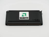
What we have here is a Slot 1 Pentium II module that has been stripped of its primary frontal heatsink, leaving only the rear plastic housing of the SECC2 (Single Edge Contact Cartridge 2) package attached.
When I flip the board over, the classic black plastic shroud is still present, complete with the molded "pentium II PROCESSOR" lettering and the genuine Intel holographic square. But the real magic is on the PCB side. Staring right at the center is the Deschutes core, still sporting a vivid blue phase-change thermal interface pad that would have historically coupled it to a massive chunk of finned aluminum. Flanking the CPU die on the right side are two massive Toshiba SRAM chips, taking up almost as much real estate as the processor itself.
Visible Identifiers & Silkscreen Transcriptions:Backplate Mold: pentium II PROCESSOR (with registered trademark)
Holographic Sticker: Present (Intel Genuine Part)
Small White Sticker: 19
CPU Die Substrate Top: 7850A048
CPU Die Substrate Bottom: 1384B.536M/F 1138
Right SRAM Chips (x2): TOSHIBA L87672 / TC55V2377AFF-225 / JAPAN 9933MBD
Edge Connector: 242-pin (Marked A1 to A121 on the visible side)
The engineering choices visible on this board represent a highly specific era in semiconductor manufacturing. In the late 1990s, L2 cache operating at core speeds was absolutely critical for performance, but it took up too much silicon space to be integrated directly into the central CPU die without destroying manufacturing yields. Intel's solution was the Slot 1 architecture. Instead of a single chip dropping into a socket, the CPU became a localized daughterboard.
The central die here is the Deschutes core, built on a 0.25-micron process. It was a die-shrink of the earlier, ridiculously hot Klamath core. Because L2 cache couldn't fit on the die, Intel placed those two Toshiba SRAM chips right next to it on this PCB. They communicated with the processor over a dedicated, tightly coupled interface known as the Back Side Bus (BSB). In the Pentium II architecture, this bus ran at exactly half the speed of the core frequency.
This specific physical package is the SECC2 iteration. The original SECC was a fully enclosed, heavy plastic and metal cassette. It was expensive to produce. With SECC2, Intel cheaped out in the smartest way possible: they kept the plastic backplate for structural rigidity and branding but left the front exposed so OEM cooler manufacturers could mount their heatsinks directly against the die and PCB.
Slot 1 is one of the most iconic physical formats in PC history. When you built a computer in this era, installing the CPU felt like locking a giant video game cartridge into an arcade cabinet. You had to physically push down with real force until the retention mechanisms clicked into place. It was incredibly satisfying.
But there was a darker, more strategic lore to Slot 1. While Intel pitched the cartridge format purely as a technical necessity for off-die L2 cache, it was also a brilliantly aggressive business move. The traditional Socket 7 standard was an open playground where rivals like AMD and Cyrix could produce chips that fit perfectly into motherboards designed for Intel processors. By patenting the Slot 1 interface, Intel effectively locked AMD out of their ecosystem, forcing AMD to engineer their own motherboards and eventually launch their own rival format known as Slot A.
Eventually, Moore's Law marched forward. By the time the Pentium III transitioned to the "Coppermine" core, transistors became small enough that Intel could finally bake the L2 cache directly into the processor die again. The giant, complex, expensive cartridge was no longer needed, and the industry happily returned to flat, socketed CPUs.
Identifying bare OEM or stripped Slot 1 processors can be slightly tricky because the S-Spec and clock speed are usually printed on the top edge of the black plastic housing. On this specific unit, that top edge is completely blank. The white barcode sticker is too worn to yield a clean part number, and the numbers on the CPU substrate (7850A048 and 1384B.536M/F) function as internal lot codes rather than public-facing identifiers.
So how do I know this is the flagship 450 MHz version? The hardware leaves a perfect breadcrumb trail through the L2 cache.
Look closely at those Toshiba SRAM chips: TC55V2377AFF-225. The "-225" suffix dictates the operating frequency of the memory, which is 225 MHz. As established in the P6 architecture rules, the Back Side Bus for a Pentium II runs at exactly half the core speed. If the cache runs at 225 MHz, multiplying that by two gives us a core speed of exactly 450 MHz.
Furthermore, the date code on these Japanese Toshiba chips is 9933, meaning they were manufactured in the 33rd week of 1999. The Deschutes 450 MHz processor launched in late 1998, but it remained heavily in production throughout 1999 as a budget alternative to the newer, significantly more expensive Pentium III Katmai cartridges. The evidence firmly cements this artifact as a late-run, top-tier Pentium II 450.