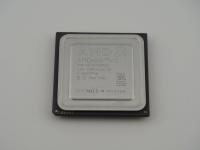
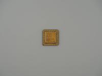
The heavy, gold-plated heat spreader sits brilliantly against the dark, purple-tinted ceramic substrate. A stunning combination of materials that feels incredibly dense and substantial in the hand, a hallmark of high-end late-nineties processor manufacturing.
Looking closely at the gold cap, the laser etching transcribes of the surface text:
AMD (Logo)
AMD-K6(TM)-2
AMD-K6-2/350AFR
2.2V CORE/3.3V I/O
A 9819FPFW
(m)(c) 1998 AMD
Designed for Microsoft Windows NT Windows 95
MALAY
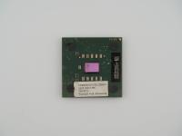
On the bottom edge of the ceramic, the numbers 26351 and the letter N are printed in a faint gold tone. More interestingly, turning the processor over reveals the staggered gold pins characteristic of the Socket 7 interface, perfectly brazed to the ceramic. The center of the pin array features a blank ceramic square that currently hosts two distinct warranty void stickers. One sticker is clearly marked with the year "2000" and features Chinese characters indicating "Warranty void if torn" alongside a grid of months. A second "Nation" sticker sits just below it. These additions give the artifact a distinct, lived-in character, pointing to a history within the bustling Asian system integrator or grey market.
Beneath that gorgeous gold cap lies the "Chomper" core. This specific piece of silicon was fabricated on a 0.25-micron process, packing approximately 9.3 million transistors.
The engineering of the K6-2 series required a split-voltage design. As indicated directly on the heat spreader, this chip requires a 2.2V core voltage and a 3.3V I/O voltage. This was a critical transition period for motherboards, requiring careful jumper configurations to avoid instantly frying the processor. Running at 350 MHz, this chip typically utilized a 100 MHz Front Side Bus (FSB) paired with a 3.5x multiplier, a configuration made possible by the Super Socket 7 standard.
The heat spreader was not just for show. The Chomper core generated a significant amount of heat for its era, and the gold-plated metal cap ensured efficient thermal transfer to the aluminum heatsinks of the day.
This is the processor that truly put AMD on the map as a fierce, uncompromising rival to Intel. Before the Athlon changed the world, the K6-2 was the guerrilla fighter of the desktop market. Built upon the architecture AMD acquired from NexGen, the K6-2 introduced 3DNow! technology. This was a custom set of SIMD (Single Instruction, Multiple Data) instructions specifically designed to accelerate floating-point math, a crucial requirement for the exploding 3D gaming market.
At the time, Intel's Pentium II was dominating, but the K6-2 offered nearly identical performance for a fraction of the cost. Furthermore, it allowed users to upgrade their existing Socket 7 motherboards, extending the lifespan of older platforms well beyond their intended obsolescence. The 3DNow! instruction set became a legendary piece of hardware lore. When game developers optimized titles like Quake II for 3DNow!, the K6-2 could actually outperform the vastly more expensive Pentium II setups. It was the ultimate underdog victory.
The identification of this piece is absolute. The surface text leaves no room for ambiguity, but breaking down the specific OPN (Ordering Part Number) AMD-K6-2/350AFR provides an exact forensic profile of this chip's tolerances.
The date code 9819 confirms this specific unit rolled off the assembly line in Malaysia during the 19th week of 1998. The presence of the year 2000 warranty stickers on the underside suggests this processor likely saw a second life, perhaps being resold or integrated into a budget build a couple of years after its initial fabrication. It is a brilliant, highly tangible piece of the late-nineties Megahertz War.