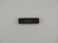
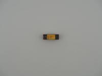
We spend so much time hunting down esoteric gold-plated mainframe modules and classified military ceramics that it is easy to forget what actually ran the world in the 1980s. This artifact is the definition of a workhorse. Sitting on the scale at exactly 6.3 grams, this is a standard plastic Dual In-line Package. It measures a standard two inches long, with forty slightly oxidized but perfectly straight pins.
Taking a close look at the top casing under the macro lens reveals the standard, slightly textured matte black resin with sharp white laser etching:
P8085AH
K910653
(m) (c) i '76 '80
Flipping it over, the mold markings on the underside tell the rest of the manufacturing story:
KOREA
I8K784  8907
The "P" prefix explicitly denotes the plastic package. The Intel lowercase "i" logo is crisp, flanked by the mask work and standard copyright symbols. The dual dates are the dead giveaway to this chip's lineage. The '76 represents the original base 8085 architecture, while the '80 points to the updated HMOS revision that this specific die utilizes.
To appreciate the 8085, you have to understand the nightmare it was designed to replace. Its predecessor, the Intel 8080, was a brilliant but needy piece of engineering. The 8080 required three separate power supplies (+5V, -5V, and +12V) just to wake up, along with a complex external clock generator and a system controller chip.
Intel engineered the 8085 to fix all of that. The "5" in 8085 literally stands for the single +5V power supply it requires to operate. They integrated the clock generator and the system controller directly onto the die. This massive reduction in external component count made it an absolute dream for engineers building embedded systems.
This specific unit features the "AH" suffix. The "A" denotes a bug-fixed stepping of the original silicon, while the "H" is where the real magic happens. It stands for HMOS (High-performance N-channel Metal-Oxide-Semiconductor). Moving from standard NMOS to HMOS allowed Intel to shrink the transistor geometries, reducing power consumption and heat generation while allowing for faster clock speeds. While the base 8085 ran at 3 MHz, the HMOS process allowed later variants to push up to 5 MHz and 6 MHz.
The history of the 8085 is a tale of winning the war but losing the battle. Intel designed it to rule the emerging desktop microcomputer market. However, a team of former Intel engineers left to form Zilog and released the Z80. The Z80 was fully compatible with 8080 code, featured a vastly superior instruction set, and completely ate Intel's lunch in the desktop space.
But the 8085 did not die. Because of its high level of integration and simple power requirements, it pivoted to become the undisputed king of embedded control systems. It ran industrial machines, microwave ovens, scientific equipment, and primitive robotics.
The ultimate flex of the 8085 architecture happened off-world. When NASA built the Mars Sojourner rover in the 1990s, they needed a processor that was utterly proven and predictable. They chose an 80C85 (the radiation-hardened CMOS variant of this exact architecture). This little 8-bit instruction set literally drove across the surface of Mars.
As a fun piece of lore, the 8085 contains a set of undocumented instructions. Intel engineers added a handful of opcodes for arithmetic and flag manipulation that they never published in the official databooks, mostly because they did not want to guarantee their compatibility in future chips. Naturally, hackers and assembly coders found them anyway and used them to shave precious bytes off their embedded programs.
Identifying this specific piece is an exercise in reading standard industry date codes. The underside stamp of 8907 indicates this chip rolled off the assembly line in Korea during the 7th week of 1989.
This date code is actually the most fascinating thing about this specific artifact. The architecture was introduced in 1976. The HMOS revision happened in 1980. The fact that Intel was still churning out massive batches of these plastic DIPs in early 1989 shows just how deeply entrenched the 8085 was in the global supply chain. By 1989, the world was moving on to the 80486 for desktop computing, yet factories were still pumping out millions of these 8-bit chips for industrial controllers and consumer electronics. It is a perfect specimen of an industry workhorse that quietly ran the background infrastructure of the late 20th century.