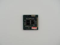
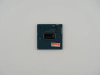
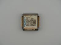
I love getting my hands on bare-die mobile silicon. Holding this piece, I immediately noticed the flawless, glossy rectangular die taking center stage. The raw aesthetic of mobile processors from this era is fantastic because there is no integrated heat spreader hiding the actual logic. Resting on the digital scale, the entire package weighs in at precisely 8.4 grams, and the ruler confirms the standard 37.5 mm square footprint of the Socket G1 platform.
Printed right onto the top edge of the substrate is the unmistakable Intel copyright and model identifier:
INTEL (m)(c) '08
i7-740QM      (e4)
SLBQG
V048A243
Flipping it over, the array of micro-PGA gold pins is pristine, leaving a distinct empty square in the center packed with tiny surface-mount capacitors. What really caught my eye is the bright red and white sticker slapped onto the front corner. It reads "核芯科技 撕毁无效" (Core Technology, void if torn) with a date field stamped for 2025. This jarring but fascinating detail tells me this chip did not just sit in a drawer. It is a salvaged warrior.
Let us talk about the heavy artillery. The Clarksfield architecture was Intel taking the incredibly successful desktop Nehalem design and cramming it into a laptop chassis. Fabricated on a 45nm process, this die packs four physical cores and eight threads thanks to Hyper-Threading.
Unlike the dual-core Arrandale chips of the same generation that utilized a messy multi-chip module (MCM) to bolt on integrated graphics, Clarksfield is pure, dedicated compute silicon. It has zero onboard graphics logic. This architecture was historically vital because it finally integrated the memory controller and the PCI Express root complex directly onto the processor die, eliminating the old front-side bus bottleneck once and for all. It chugged along at a base clockspeed of 1.73 GHz, but when thermals allowed, Intel's aggressive Turbo Boost could push a single core all the way up to 2.93 GHz. Handling all of this logic inside a laptop required a 45W Thermal Design Power rating.
In 2010, if you bought a massive, back-breaking gaming laptop or a mobile workstation, the Core i7-740QM is likely what powered it. I am talking about the legendary thick Alienwares and Asus Republic of Gamers bricks.
The lore around these chips always centers on their thermal output. They ran scorchingly hot. Because it lacked an integrated GPU, laptop manufacturers were forced to pair it with dedicated Nvidia or AMD graphics, meaning the cooling systems had to dissipate massive amounts of heat from two separate, power-hungry dies. Battery life was practically non-existent. You did not buy a 740QM machine to work on an airplane. You bought it to plug into a wall and dominate desktop users at LAN parties. It was brute force engineering at its finest.
The physical evidence is entirely locked in. The SLBQG S-Spec specifically confirms this is the OEM and retail stepping for the i7-740QM processor. The batch code V048A243 perfectly aligns with the manufacturing windows of 2010.
The true story of this specific artifact lies in that red Chinese warranty sticker. It proves this chip lived a full life in a high-end machine before being harvested at an e-waste or refurbishing facility in Shenzhen or a similar tech hub. It was ripped from a dead motherboard, tested, slapped with a modern 2025 warranty seal, and thrown back into the wild for a second life. It is a fantastic piece of grey-market hardware history sitting right on the bench.