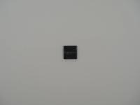
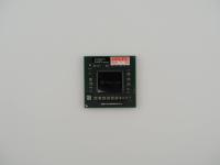
When examining the surface of this specific unit, the contrast of the laser etching against the matte black epoxy resin is remarkably sharp. Here is the exact surface transcription pulled from the top mold:
(Top Row, Inverted): APL0498 339S0184
(Left, Vertical): VTLJ2807H8 1306
(Center): [Apple Logo] A5
(Right, Vertical): H9TKNNN4KDAPYR-NDM
(Bottom): N52FR021 1310
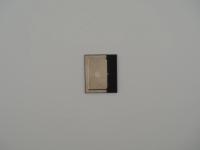
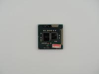
The top surface is a monolithic slab of black molding compound. Flipping the artifact over reveals a dense, tightly pitched BGA (Ball Grid Array) pad layout on a deep green organic substrate. The pads are bare, indicating this SoC was either expertly desoldered or never mounted to a mainboard. The aesthetic is purely functional, a tiny dark square that completely altered the trajectory of modern computing.
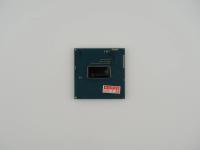
The APL0498 silicon die is a fascinating piece of early 2010s engineering. This is a Package-on-Package (PoP) module. The black square we are looking at is not just a CPU. It is a multi-layered sandwich. The bottom layer, connecting directly to the BGA pads on the underside, is the main SoC die fabricated by Samsung Electronics on their 45nm process node.
The vertical text on the right side reading H9TKNNN4KDAPYR-NDM is the crucial engineering giveaway. That is an SK Hynix part number for a 4-Gigabit (512 MB) LPDDR2 mobile memory module. To save precious motherboard real estate inside the tightly packed chassis of early smartphones and tablets, Apple and their fabrication partners stacked the RAM directly on top of the logic die inside the same epoxy package.
At its core, the A5 utilizes a dual-core ARM Cortex-A9 processor alongside a dual-core PowerVR SGX543MP2 GPU. The thermal characteristics were incredibly aggressive for the time. This chip had to run completely passively cooled inside a glass and metal enclosure while delivering roughly twice the CPU power and nine times the graphical performance of its predecessor, the A4.
The Apple A5 is a titan of mobile computing history. It debuted in the iPad 2 in March 2011 and subsequently powered the iPhone 4S. It is the chip that made Siri possible. The heavy natural language processing overhead required for the original Siri launch relied heavily on the A5's dual-core architecture.
In the collector community, the A5 is often jokingly referred to as the cockroach of Apple silicon. It refused to die. Apple kept this architecture alive across multiple product lines for years, including the first iPad Mini, the 3rd generation Apple TV, and the 5th generation iPod Touch. Because it was integrated into so many long-lasting devices, it became a massive bottleneck for iOS developers. Software engineers had to continuously optimize modern iOS updates to run on this aging 45nm architecture, a testament to just how widely deployed this specific piece of silicon actually was.
Identifying this artifact is an absolute certainty based on the visible surface codes. The APL0498 designation completely isolates this as the original 45nm fabrication of the A5. Apple later released die-shrunk 32nm versions designated as the APL2498 and APL7498, but the unit in my hand is the original heavy-hitter.
What makes this specific unit highly interesting to me is the date code printed at the very bottom: 1310. In the semiconductor world, this translates to the 10th week of 2013. The A5 originally launched in early 2011. Finding an original 45nm APL0498 fabricated in early 2013 points to an interesting piece of supply chain history. By 2013, Apple had already introduced the iPhone 5 with the A6 chip. However, they continued selling the iPhone 4S as a budget 8GB model for years in developing markets and as an entry-level tier. This 2013-stamped A5 was almost certainly destined for one of those late-run budget iPhone 4S units, fresh off the Samsung fab lines long after the flagship spotlight had moved on.