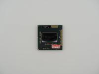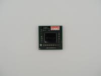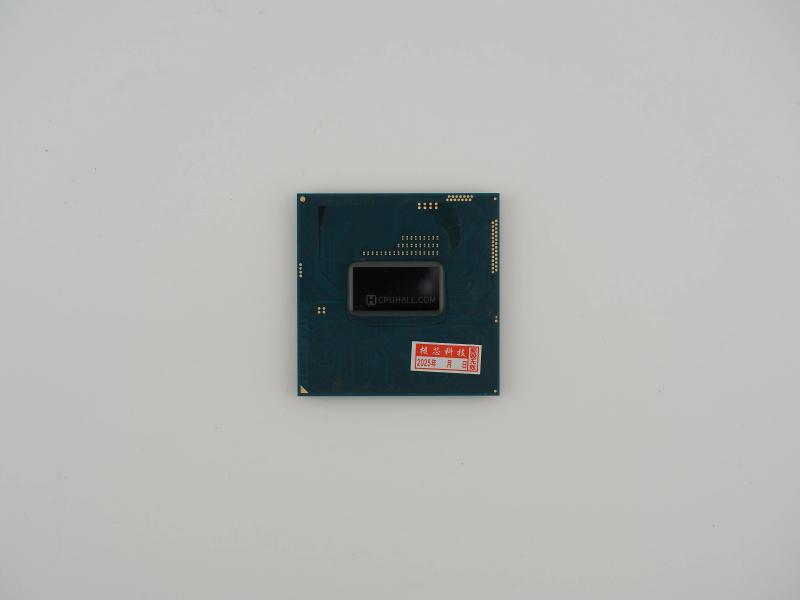

Holding this piece, the first thing that strikes me is the mirror-like finish of the naked silicon. Without an integrated heat spreader to block the view, we get to look directly at the compute die mounted to the classic industrial green fiberglass substrate.
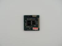
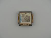
Placing this artifact on the scale, it registers exactly 6.1 grams. Against the ruler, it measures right around 37.5 by 37.5 millimeters. Flipping it over reveals the gold pin grid array. Unlike desktop processors which often feature longer pins, these mobile rPGA pins are incredibly short and stout. They almost look like flat solder balls until you get them under a macro lens and see the distinct cylindrical structure and offset grid pattern.
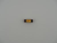
Visible Markings Transcribed:Left Edge: G66143 01 IB5
Top Left: V307... (Faint FPO batch code)
Sticker: 核芯科技 (Core Technology) / 2025年 月 日 撕毁无效 (Void if torn)
Bottom: SR1HF
The vibrant red sticker on the lower right is a fantastic touch of modern hardware archaeology. It is a warranty void tag from a Chinese electronics recycler. This tells me this chip was ripped out of a dead laptop, cleaned, tested, and marked for resale in the Shenzhen secondary markets. It gives the artifact a distinctly gritty, salvaged aesthetic.
This architecture represents a massive shift in Intel's power delivery philosophy. Built on the 22nm FinFET process, Haswell was the "Tock" in Intel's manufacturing cycle. But the real engineering magic here is the Fully Integrated Voltage Regulator (FIVR).
Prior to this generation, motherboard manufacturers had to build complex voltage regulation modules around the CPU socket. With Haswell, Intel moved those power delivery components directly onto the processor package itself. This drastically simplified laptop motherboard designs and allowed the chip to control its own power states with incredibly fine granularity. The tradeoff was that all that voltage conversion generated extra heat on the die, making these bare-silicon mobile chips notoriously tricky to keep cool inside thin plastic laptop chassis.
This specific family of chips represents the twilight of an absolute golden era for laptop enthusiasts. Haswell and Socket G3 marked the final generation where upgradeable, socketed processors were the standard for mainstream notebooks.
If you bought a cheap laptop with a dual-core Celeron 2950M back in 2013, you could theoretically open the chassis, twist the socket lock with a flathead screwdriver, and drop in a massive Core i7 quad-core beast. After this generation, Intel forced the mobile computing industry aggressively toward soldered BGA packaging. The era of the easily upgradeable laptop CPU effectively died here. Holding this socketed mobile chip feels like holding a relic from a time when consumers actually owned their hardware and had the right to tinker with it.
The printed identifier G66143 on the left edge of the substrate and the S-Spec SR1HF on the bottom right of the substrate is the smoking gun. That specific part number is the definitive Intel PCB identifier for Haswell mobile processors built for Socket G3 (rPGA-946B).
The ruler confirms the standard 37.7mm square dimensions of that exact socket. The pinout array perfectly matches the Haswell socket layout, completely ruling out older Ivy Bridge or newer Broadwell designs. Finally, the elongated rectangular shape of the silicon die is characteristic of Intel's dual-core Haswell layout.