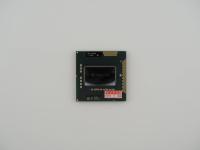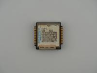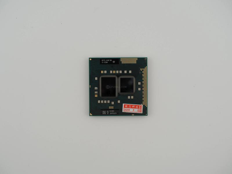
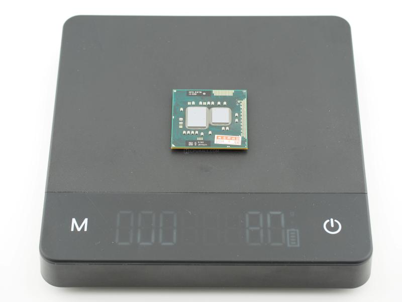
Holding this specific unit in my hand, I immediately notice the visual story told by its surface. This artifact weighs exactly 8.0 grams on the scale and measures roughly 37.5mm square. The front reveals a classic multi-chip module layout with two distinct, mirrored bare silicon dies mounted on a green organic substrate. The dark silicon has faint surface micro-scratches from a previous life inside a heavily used laptop chassis. I love looking at the contrast between the highly reflective die surfaces and the matte green board.
The laser-etched text is perfectly legible upon close inspection:
Top Left Etching:INTEL (m)(c) '08
i5-520M (e4)
Left Edge Etching:E44701 01 IB4
Bottom Barcode Label:4294
SLBU3
J049D624
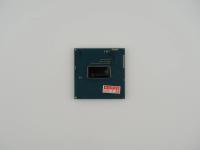
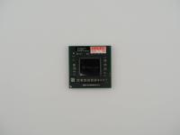
What I find incredibly amusing is the aftermarket sticker placed somewhat carelessly on the bottom right of the substrate. It is printed in bright orange and reads "核芯科技 撕毁无效 2025年 月 日" which translates to "Core Technology, Void if torn, 2025". This little piece of paper tells us exactly where this chip has been recently. Flipping the artifact over reveals the dense gold pin field of the PGA-988 package. The completely bare central island is populated only by surface-mount decoupling capacitors. The pins themselves show minor signs of oxidation but remain remarkably straight.
Let us dive into the engineering of the Arrandale architecture. This chip represents a very specific, slightly awkward teenage phase in Intel processor design. The physical artifact is a Multi-Chip Module (MCM). The smaller die on the right side of the package is actually the 32nm CPU logic containing two cores and four threads. The notably larger die on the left is the 45nm Iron Lake Graphics and Memory Controller Hub.
Intel could not quite fit everything onto a single monolithic piece of silicon on their brand new 32nm fabrication node just yet. They essentially glued a motherboard northbridge and a CPU core together on the same package and connected them via an internal QPI link. It runs at a base clockspeed of 2.4 GHz but can aggressively turbo up to 2.93 GHz when thermals allow. To cool this dual-die setup, laptop manufacturers had to use large copper cold plates and thermal paste applied across both bare silicon rectangles. This often led to messy, uneven mounting pressure from factory assembly lines.
The legacy of the i5-520M is one of sheer corporate ubiquity. If you worked in a modern office between 2010 and 2013, you almost certainly typed on a heavy, notoriously hot ThinkPad or Dell Latitude powered by this exact piece of silicon. It was the mainstream champion of the "First Generation Core" series.
The lore here is not about supercomputers or cold war secrets. It is about the brutal march of Moore's Law. This MCM design was a stopgap measure. Just one year later, Intel released the legendary Sandy Bridge architecture and fully merged the GPU and CPU into a single monolithic die. The Arrandale architecture was rendered instantly obsolete by the march of progress. It is genuinely funny to look back at these disjointed MCM designs now that modern processors have entirely returned to using modular chiplets. Arrandale was doing chiplets before it was considered cool or highly efficient.
Provenance for this artifact is wonderfully mundane yet highly specific. I did not pull this from a secret underground vault. The SLBU3 S-Spec strictly identifies it as an OEM processor meant for socketed laptops. The visual evidence of the Chinese warranty sticker completely gives away its recent history.
This unit was stripped out of a dead enterprise laptop, bulk shipped to an electronics recycling hub in Shenzhen or a similar industrial tech market, tested, slapped with a warranty sticker valid through the year 2025, and resold on the secondary market. It is a hardened survivor of the massive global e-waste ecosystem. It stands proudly in the collection not as a crown jewel of rarity, but as a monument to the staggering scale of early 21st-century global computing.