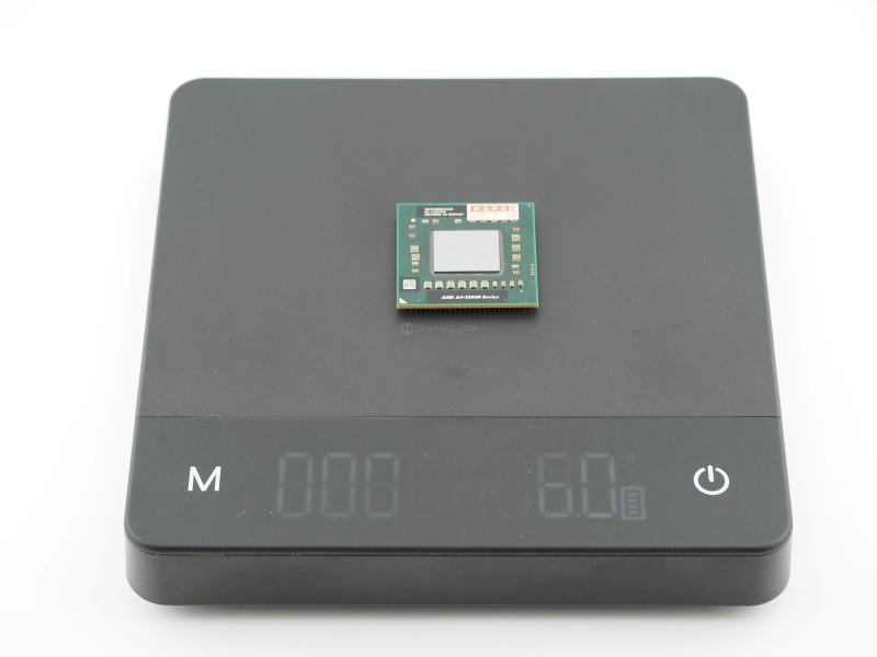
When I drop this little slice of silicon on the precision scale, it registers a mere 6.0 grams. It is incredibly light, completely mundane, and yet physically dense. Looking at the bare die resting on its green fiberglass substrate, the reflection is glassy and perfect. We do not have a heat spreader here, which is typical for mobile parts, meaning the silicon itself had to take the direct mounting pressure of whatever cheap laptop cooling assembly it was originally strapped to.
Under the macro lens, the surface text is clearly legible against the black organic material beside the die:
AM3300DDX23GX
DA 1124CPM
DIFFUSED IN GERMANY

AMD A4-3300M Series
Flipping this artifact over reveals the 722 gold-plated pins of the micro-PGA layout. They are pristine. I always check the corners on these older mobile PGA chips because careless laptop teardowns usually result in bent or sheared pins, but this specific unit is flawless. The most glaring physical trait, however, is not the silicon itself. It is that bright red paper sticker stubbornly adhered to the top edge. It reads "核芯科技" (Core Technology) with a void-if-removed warning and a date printed for the year 2025. It is a fantastic piece of visual dissonance, a cheap aftermarket warranty tag slapped onto a chip fabricated over a decade ago.
This chip represents the realization of a massive gamble. The A4-3300M is based on the Llano core, part of AMD's very first generation of true APUs. This is a 32nm Silicon-on-Insulator (SOI) part that was manufactured by GlobalFoundries in Dresden, Germany.
Technically speaking, we are looking at two modified "Husky" K10 x86 processing cores running at a base clock of 1.9 GHz. But the x86 cores are only half the story. The rest of that mirrored die is dedicated to a TeraScale 2 architecture GPU, specifically the Radeon HD 6480G packing 240 unified shaders.
Fitting both a CPU and a highly capable integrated GPU on a single die with a 35W TDP was a serious thermal and architectural challenge in 2011. AMD had to rip out the L3 cache entirely just to make room for the graphics compute units. To compensate, they doubled the L2 cache to 1MB per core. The pin layout for Socket FS1 had to route not just memory and PCIe lanes, but also handle the complex power delivery needed to dynamically shift voltages between the CPU block and the GPU block depending on the user's workload.
This little square of green fiberglass is the direct descendant of AMD's multi-billion dollar acquisition of ATI in 2006. For years, AMD hyped the "Fusion" project. The idea was simple but revolutionary: strap a capable graphics processor and a CPU together on the same die. By the time Llano finally hit the market in the summer of 2011, it was heavily delayed and plagued by terrible initial 32nm yields at GlobalFoundries.
As a high-end collector, I do not display this chip because it was a performance monster. It absolutely was not. Intel's Sandy Bridge architecture was released around the same time and completely obliterated the A4-3300M in raw CPU processing power. However, Intel's integrated graphics were notoriously abysmal. AMD's Llano chips dominated in graphical tasks. This humble piece of silicon proved that the APU concept worked. It paved the immediate path for AMD to secure the contracts for the PlayStation 4 and Xbox One consoles, single-handedly saving the company from bankruptcy during their darkest years.
Identifying this piece is straightforward thanks to the legible OPN (AM3300DDX23GX). The date code 1124 confirms this specific unit was assembled in week 24 of 2011.
The true story of this specific artifact lies in that red Chinese vendor sticker. You do not see 2025 warranty expiration dates on 2011 hardware unless it has been aggressively recycled. Millions of cheap, low-end laptops featuring this exact APU flooded the global market. Over the years, those laptops died, their hinges broke, and their batteries swelled. They were shipped by the container load to e-waste recycling hubs in Shenzhen. Someone carefully desoldered or unlocked the socket, extracted this A4-3300M, cleaned off the thermal paste, slapped their own "Core Technology" shop sticker on it, and threw it into a bin to be sold as a replacement part for a few pennies. It is a perfect specimen of the global silicon aftermarket lifecycle.