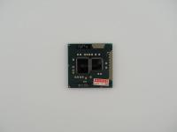
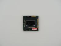
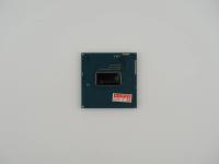
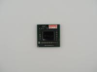
Holding these chips, I immediately notice the familiar feel of mid-2000s Intel mobile silicon. The green organic substrate and the exposed, mirror-like rectangular die are classic hallmarks of the era before integrated heat spreaders became standard on mobile parts. I actually have two distinct units, both carrying the exact same S-Spec, weighing in at a mere 6.0 grams.
Let us transcribe the surface text directly from the artifacts:
Unit Top Markings:LF80539 T2500
7712A440 SL9EH
Die-Edge Markings):2.00/2M/667
INTEL (M) (C) 04 (e4)
Flipping the package over reveals a dense field of 478 gold-plated pins designed for the Socket M interface, missing just two pins in one corner for socket orientation. Notably, both of these units feature a brightly colored tamper sticker reading "盛芯国际 2025年" (Shengxin International 2025). This is a clear indicator that these specific artifacts were recently pulled from bulk e-waste recycling operations in Shenzhen and tested for resale. It gives the silicon a gritty, second-life aesthetic that I always appreciate in salvaged hardware.
Under the hood, this is the Yonah architecture. It represents a massive pivot in semiconductor design for Intel. Built on a 65nm manufacturing process, Intel managed to pack 151 million transistors into a tiny 90 square millimeter die. The laser etching 2.00/2M/667 perfectly summarizes the raw specifications. We are looking at a 2.0 GHz clock speed, 2 Megabytes of shared L2 cache, and a 667 MHz Front Side Bus.
The shared L2 cache, branded internally as Intel Advanced Smart Cache, was a brilliant piece of engineering for the time. Unlike earlier desktop dual-core chips like the Pentium D which simply bolted two distinct Pentium 4 silicon dies onto one package, Yonah was a native dual-core processor. Both execution cores could dynamically allocate cache memory based on the immediate workload. If one core was idling, the active core could commandeer the full 2MB of cache. This, combined with aggressive power gating that allowed unused portions of the chip to power down, kept the Thermal Design Power (TDP) to a highly manageable 31 watts.
The historical weight of the Core Duo cannot be overstated. While desktop users were suffering through the blistering heat and massive power draw of the NetBurst Pentium 4 era, Intel's mobile design team in Haifa, Israel, was quietly building the future. They took the highly efficient Pentium M architecture and evolved it into Yonah. This is the chip that finally killed the Pentium brand as Intel's flagship product. It launched the "Core" nomenclature that continues to dominate the industry today.
Even more historically significant, this exact model (the 2.0 GHz T2500) was the beating heart of the very first Intel-based Apple MacBook Pro, announced by Steve Jobs in January 2006. Apple was transitioning away from PowerPC precisely because IBM and Motorola could not deliver a cool, efficient G5 processor for laptops. Yonah was the silver bullet Apple needed. It literally shifted the landscape of personal computing.
The only strange historical quirk of this processor is its instruction set. Despite launching in early 2006 when AMD had been championing 64-bit computing for years, Yonah was strictly a 32-bit processor. Intel would not bring 64-bit (EM64T) to their mobile line until the Merom architecture arrived a few months later as the "Core 2 Duo".
There is absolutely zero mystery regarding the identity of these chips, but examining the batch codes reveals a bit of their specific timeline. The S-Spec SL9EH confirms these are the standard OEM/retail PGA versions of the T2500, not BGA chips meant to be soldered directly to a motherboard.
The FPO (Finished Process Order) codes 7719A463 and 7712A440 tell me exactly when these were born. The first digit "7" indicates the year 2007, and the following two digits "19" and "12" indicate the week of manufacture. The copyright date of 04 on the die edge relates to the underlying mask copyright year, not the physical production year. Seeing these chips stripped from whatever high-end business laptops they originally powered is a humbling reminder of tech lifecycle. It is just a small square of green fiberglass and silicon, but it represents the exact moment Intel stopped chasing megahertz and started prioritizing performance per watt.