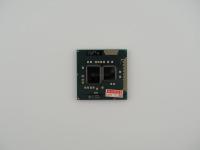
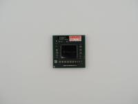
Holding this piece in the lab, I am immediately struck by how utterly standard it feels, yet how much history is crammed into a 35mm square. Placing it on the scale, it registers a feather-light 5.9 grams. The top features an exposed, mirror-finish silicon die flanked by a chaotic mix of laser-etched markings and aftermarket vendor stickers.
Surface Transcriptions:Top Edge: LF80539 T2400
Top Edge: 5616A784 SL8VQ
Bottom Edge: 1.83/2M/667
Bottom Edge: INTEL (M)(C)04 (e4)
Vendor Sticker 1: 小彬 CPU (Xiao Bin CPU) with date matrix
Vendor Sticker 2: 1S41A1014ZVQ01J66F2PV W1134 606
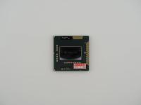
Flipping this artifact over reveals the dense gold grid of the PGA-478 interface. The pins are immaculate. I absolutely love the blue Chinese vendor sticker plastered right next to the die. It screams "Shenzhen electronics market." This chip was likely harvested from a dead laptop, tested, slapped with a warranty void sticker, and resold to keep another machine breathing. The (e4) marking on the resin indicates it is a lead-free, RoHS-compliant component.
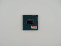
This is the Yonah architecture in its purest form. Underneath that tiny exposed die sits 151 million transistors fabricated on Intel's 65nm process. What makes this chip fascinating is the thermal envelope. It has a Thermal Design Power of just 31 Watts.
The engineering leap here was the Smart Cache. Instead of each core having its own isolated pool of L2 cache, Intel designed a shared 2MB L2 cache. If one core was idle, the other core could commandeer the entire 2MB. This was a massive paradigm shift for mobile efficiency. It communicates with the rest of the system over a 667 MHz Front Side Bus. Notably, this is a 32-bit only processor. It lacks the Intel 64 instruction set, which would become the standard shortly after with the Core 2 series.
If you look at this little green square and just see e-waste, you are missing one of the most pivotal moments in computing history. Prior to this, Intel was trying to shove the Pentium 4 architecture into laptops. Those NetBurst chips were literal lap-scorchers. They guzzled battery life and required massive copper heatsinks. Intel needed a miracle, and the Israeli design team in Haifa delivered Yonah.
This specific silicon is legendary for one massive reason. When Steve Jobs stood on stage in 2006 and announced Apple was abandoning PowerPC to transition to Intel, the Core Duo was the spearhead. The original 15-inch MacBook Pro and the first white polycarbonate MacBooks were powered by chips exactly like this T2400. It effectively ended the megahertz myth and proved that instruction-per-clock efficiency was the true path forward for mobile computing. It was a massive victory for Intel and a death blow to IBM's mobile PowerPC ambitions.
Identification of this artifact is rock solid based on the surface etchings. The S-Spec SL8VQ perfectly correlates to the Intel Core Duo T2400.
I can even trace its exact birthday. Reading the FPO batch code 5616A784, the 5 indicates the manufacturing plant, the 6 stands for the year 2006, and the 16 means it rolled off the fabrication line in the 16th week of that year. The LF prefix on the part number explicitly denotes the Lead-Free packaging. The barcode stickers confirm it was pulled by a large-scale system refurbisher before making its way into my hands. It is a perfectly documented piece of mid-2000s silicon history.