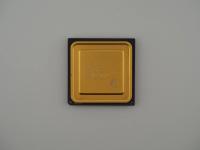
In an era dominated by Intel's standard grey and dark brown ceramic, this rich purple hue became a signature visual identifier for early alternative silicon manufacturers.
Dropping it onto the museum scale, it registers at precisely 7.4 grams of computing history. Turning the artifact over reveals a stunning layout. The 68 gold-plated pins are arranged in a dual-ring outer perimeter, flanking a prominent, brazed gold center pad. This central pad acts as a heat spreader, a necessary addition for the thermal demands of late-1980s high-speed logic.
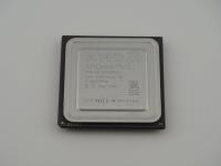
The surface markings are highly legible, and I was able to transcribe the following from the top face:
[IIT Logo] IIT
3C87 -25
(M)(C) IIT 1988
1002BC3C1F0C
A1A1
ID 91053D USA
Adding a beautiful layer of organic provenance to this specific unit is the torn paper warranty sticker. It reads 18.6.91. This is a classic European or international date format for June 18, 1991, indicating exactly when this coprocessor was installed into a motherboard by a system builder or retailer.
Before the 486DX integrated floating-point logic directly into the main processor core, complex math was an optional luxury. The 80386 CPU was strictly an integer machine. If a user wanted to run early 3D rendering software, intensive CAD programs, or massive financial spreadsheets, they had to drop a dedicated FPU (Floating Point Unit) into the empty socket sitting next to the main processor.
The IIT 3C87-25 is a math coprocessor designed to interface directly with an Intel or AMD 386 CPU running at a matching 25 MHz front-side bus. But this chip is completely unique under the hood. Founded by former Intel and Motorola engineers, IIT did not just reverse-engineer Intel's design. They built a clean-room implementation that was fundamentally superior.
Intel's standard 80387 utilized an 8-register floating-point stack. IIT engineers radically expanded this, designing the 3C87 with 31 internal registers. By minimizing the time spent shuffling data in and out of the FPU, the 3C87 could execute identical floating-point instructions significantly faster than Intel's official chip. Furthermore, IIT integrated specialized hardware to accelerate 4x4 matrix transformations. This was an incredibly forward-thinking feature designed specifically to accelerate 3D graphics calculation, predicting the necessity of the GPU years before the concept existed.
This little purple square is a veteran of the Great Clone Wars of the late 1980s and early 1990s. Intel was charging exorbitant prices for their math coprocessors, sometimes asking as much as the main CPU itself. Companies like Cyrix, ULSI, and IIT smelled blood in the water.
IIT's aggressive marketing and superior performance terrified Intel. The lore of the era is filled with aggressive benchmark wars and legal battles. Intel frequently attempted to scare consumers by claiming third-party coprocessors were incompatible or prone to calculation errors. In reality, the IIT chips were rock solid.
The tragic irony of the IIT 3C87 lies in its most brilliant feature. The dedicated 4x4 matrix multiplication instruction was a stroke of genius, but because Intel's official chip did not possess this instruction, almost no software developers ever wrote code to take advantage of it. It remains a fascinating what-if in the history of 3D graphics acceleration.
Analyzing the surface codes gives us a perfect timeline of this artifact's life cycle. The copyright reads 1988, which aligns with the initial architectural tape-out and intellectual property filing for the IIT FPU design.
However, the specific manufacturing codes tell a later story. The bottom laser etching ID 91053D contains a standard date code format. The 9105 indicates this specific piece of silicon was packaged in the 5th week of 1991 (late January or early February).
The journey of this chip is completely verified by the paper sticker. Manufactured in early 1991, it was shipped to a distributor, sold to a system builder, and slapped with a warranty seal on June 18, 1991, before being seated into a high-end 386 workstation. The USA stamping indicates the final packaging or testing location, though the actual silicon wafer was likely fabbed elsewhere. The A1A1 stepping code suggests this is an early, highly refined revision of the 25 MHz silicon.