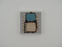
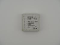
As documented on the scale, this specific artifact weighs a staggering 139.3 grams. For context, a modern desktop CPU feels like a hollow plastic toy compared to this. It feels less like a computing component and more like a beautifully machined slab of tank armor.
The front of the processor is dominated by a monolithic, completely flat metallic Integrated Heat Spreader (IHS). Unlike consumer chips that feature stylized logos, this artifact is strictly business. The surface is completely bare except for a few crisp laser etchings and a pair of 2D datamatrix barcodes used for internal factory tracking.
Here is the exact surface transcription decoded under macro lighting:
00LT112
9DBET00C05 9316 CA P
VH3932184872
1
When looking at the back of this board, the transition from vintage to modern engineering is glaringly obvious. Peeking out from the edges of the metallic lid is a dark green organic build-up substrate measuring approximately 68x68mm. Flipping it over reveals an absolute sea of thousands of gold Land Grid Array (LGA) pads. The density is mesmerizing. The pad array is bisected down the dead center by a thick, unpopulated channel. This is a signature power delivery and routing design choice for IBM heavy-iron processors of this era.
Diving into the technical weeds of this silicon is where things get truly absurd. The IBM POWER8 module is a marvel of 22nm Silicon on Insulator (SOI) fabrication technology.
IBM engineers packed roughly 4.2 billion transistors into the 650-square-millimeter die sitting underneath that massive heatspreader. The architecture was designed to be massively multithreaded. A fully unlocked 12-core POWER8 chip is capable of handling eight hardware threads per core, meaning a single piece of silicon could execute 96 threads simultaneously.
To feed a chip running at such extreme throughput, the memory subsystem had to be entirely rethought. The POWER8 chips featured massive pools of embedded DRAM (eDRAM) directly on the module to serve as colossal L3 caches, ensuring the cores were never starved for data during mission-critical database operations. The thermal challenges of running a chip like this are precisely why the heatspreader is so ridiculously thick and heavy. This 139-gram slab of metal is engineered to absorb and spread thermal energy fast enough to be whisked away by high-RPM server fans.
The legacy of the POWER8 architecture is heavily tied to the OpenPOWER Foundation. IBM realized that fighting the Intel Xeon juggernaut alone was a losing battle. Their solution was to open up the POWER architecture, allowing other hardware vendors to build compatible servers, accelerators, and network devices.
One of the coolest architectural quirks introduced here was the Coherent Accelerator Processor Interface (CAPI). This allowed external hardware accelerators to talk directly to the CPU cache, bypassing traditional PCIe bottlenecks. It was a forward-thinking move that set the stage for modern AI and supercomputing workloads.
A common myth is that because these are organic substrates, they are fragile compared to the ceramic chips of the past. Holding this specific artifact completely dispels that notion. The substrate is remarkably rigid, reinforced by the absolute structural integrity of the metallic lid.
Identifying modern IBM silicon requires a forensic approach to internal FRU (Field Replaceable Unit) codes, as IBM rarely prints clear marketing names on their hardware.
The 00LT112 string etched on the heatspreader is a definitive internal identifier for the IBM Power family. Furthermore, similar modules bearing the 9DBET batch code and 9316 date markings frequently map to 12-core POWER8 parts running around 3.02 GHz, typically pulled from massive scale-up enterprise boxes like the Power Systems E870 or E880. The undeniable weight, scale, and specific LGA pad layout point directly to the heart of an IBM Power System machine. The physical and forensic evidence is conclusive: this is a definitive piece of POWER8 architecture.