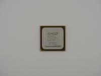
Weighing in at exactly 81.5 grams, this thick slab of white ceramic feels less like a traditional computer component and more like a piece of structural architecture. Looking closely at the top surface, the visual contrast between the two massive bare silicon dies is absolutely striking.
The smaller, completely flat metallic square die located at the bottom is the primary logic processor. However, the true visual standout is the massive rectangular die situated directly above it. Under direct light, this upper die reflects a stunning, iridescent blue and green geometric pattern. You can actually see the macroscopic layout of the memory arrays physically etched across the silicon. Both of these massive logic blocks are permanently anchored to the ceramic substrate with a thick, glossy black epoxy underfill to prevent mechanical shearing under extreme thermal expansion.
Scanning the top edge, positioned right next to a flawless row of brazed gold surface-mount capacitors, we find a very faint laser-etched sequence:
96P3675
Flipping this specific unit over tells a story of heavy use. The entire underside is caked in heavily smeared, oxidized silver thermal paste. This metallic residue completely obscures the delicate Land Grid Array pads beneath it. It is a messy, visceral badge of honor that serves as a reminder of the massive thermal loads this chip generated in the server room.
The IBM POWER5 architecture was an unapologetic, brute-force approach to enterprise processing. Fabricated on a 130nm copper Silicon-on-Insulator (SOI) process, this chip was engineered to handle relentless transactional workloads.
The magic of this specific component lies in its structural layout. The smaller logic die contains two physical execution cores alongside 1.9MB of L2 cache, built out of roughly 276 million transistors. But the beautiful, iridescent rectangular die above it is what gave this processor its true power. That separate slab of silicon is an enormous 36MB L3 cache built entirely out of eDRAM (embedded DRAM). By moving this massive cache off the main processor die but keeping it on the exact same physical package, IBM managed to bypass the brutal latency bottlenecks of accessing main system memory. The internal traces buried inside the thick white ceramic handle the ultra-high-bandwidth communication between the two dies.
This chip was also IBM's grand introduction to Simultaneous Multi-Threading (SMT) in the POWER lineage. Each physical core could execute two threads at exactly the same time, making this single dual-die slab appear as four distinct logical processors to the operating system.
The mid-2000s server market was an absolute bloodbath, and the POWER5 was IBM's heavy artillery. While Intel was struggling desperately to convince the enterprise world that the Itanium architecture was the future, IBM was quietly dropping these ceramic bricks into their System p5 mainframes and completely destroying database benchmarks.
There is a fantastic piece of lore among big iron system administrators regarding this specific generation of chips. The rumor is that IBM engineers over-architected the POWER5 execution pipelines to such a ludicrous degree that the cores frequently ran out of raw data to chew on. The logic was simply too fast for standard memory topologies. As a result, the massive external eDRAM cache die was not just a luxury; it was practically mandatory just to keep the processor from idling while waiting for the hard drives to spin. This chip represents the absolute zenith of the "big iron" philosophy. It was not designed to be cheap, and it certainly was not designed to run cool.
Collectors often get tangled up trying to identify chips from this era because IBM produced so many wild variations of the architecture. You will frequently see massive 8-die Multi-Chip Modules (MCM) the size of a dinner plate, as well as the later Quad-Chip Modules (QCM) introduced with the die-shrunk POWER5+.
So, what exactly is this specific artifact? I can definitively confirm that this is a standard IBM POWER5 DCM (Dual-Chip Module).
The physical layout tells the entire story without requiring a boot sequence. The presence of exactly one central processor die paired directly with exactly one L3 eDRAM die on a shared ceramic substrate is the universal, unmistakable fingerprint of an IBM Dual-Chip Module. Furthermore, cross-referencing the faint laser-etched 96P3675 part number against vintage IBM Field Replaceable Unit (FRU) catalogs locks in this identity. This part number explicitly maps to the original 130nm POWER5 logic units used in standard System p5 rack servers, cleanly separating it from the later 90nm POWER5+ revisions. It is a textbook, perfectly preserved example of a true mid-2000s enterprise workhorse.