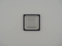
Handling this artifact gives a real sense of early 2000s server engineering. Looking closely at the top, the micro-contrast reveals significant scuffing on the metal, indicating this chip may have lived a hard life under a heavy heatsink before being decommissioned.
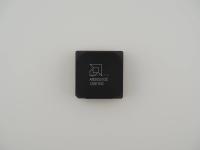
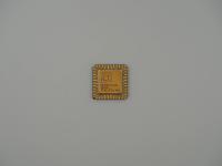
The laser etching on the surface is completely intact and reads:
AMD-8131™
AMD-8131BLC
B1 0401BQB 2
© AMD 2001
ASSEMBLED IN TAIWAN
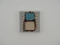
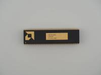
Flipping this specific unit over reveals a dense, beautifully uniform Ball Grid Array (BGA) package. The organic brown substrate is classic for the era. The solder balls are still remarkably pristine, reflecting the studio lights perfectly. It is a dense array meant for a permanent, high-reliability connection directly to a multi-processor server motherboard.
This is not a central processing unit. The AMD-8131 is a PCI-X Tunnel, a highly specialized chipset component. To understand its purpose, you have to look at the architecture of early enterprise servers.
The AMD Opteron processor used a revolutionary high-speed, point-to-point interconnect called HyperTransport. However, enterprise environments needed to connect massive, bandwidth-hungry expansion cards like hardware RAID controllers and multi-port Gigabit Ethernet adapters. Those cards used the PCI-X standard. The AMD-8131 served as the critical bridge between the CPU's HyperTransport link and the physical PCI-X slots on the board.
It supported two independent PCI-X bridges, operating at up to 133 MHz with a 64-bit wide bus. Moving that volume of parallel data takes serious electrical signaling power, which explains why a mere "bridge" chip required such a substantial metal heat spreader to manage the thermal load.
This seemingly mundane piece of silicon represents a pivotal moment in computing history. The AMD-8000 series chipset, which included this 8131 tunnel and the 8111 I/O hub, was the unsung hero of the Opteron revolution.
When AMD launched the K8 architecture, they caught Intel completely off guard. By moving the memory controller directly onto the CPU die and utilizing HyperTransport for I/O, AMD eliminated the traditional "front-side bus" bottleneck. But all that CPU power meant nothing if the server could not talk to its storage arrays fast enough. The AMD-8131 was the heavy lifter that ensured the Opteron could actually ingest data as fast as it could process it. It was the backbone of systems built by Sun Microsystems, IBM, and HP during AMD's golden era in the data center.
The identification of this artifact is rock solid. The surface markings provide a perfect forensic trail.
While the copyright explicitly states 2001, the date code on the third line reads 0401. In semiconductor manufacturing standard formatting, this indicates the chip was physically packaged in the first week of 2004. This aligns perfectly with the explosive rollout of enterprise Opteron hardware across the globe. The BLC suffix in the part number denotes the specific stepping and package revision of the silicon. It is a fantastic, raw example of the infrastructure that powered the early 2000s web.