Holding this piece is a striking reminder of when computing hardware was physically imposing. Tipping the scales at exactly 212.0 grams and measuring roughly 24 centimeters across, this board is a dense slab of late 1980s engineering.
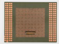
Shooting this under my 45mm Elmarit macro lens reveals an incredible level of high-fidelity detail. The micro-contrast on the central ceramic package is phenomenal. The white ceramic substrate is pristine, but the real star is the brilliant gold lid. The reflections off the gold cap highlight the meticulous brazing process used to seal the die. It is a stunning, museum-grade aesthetic that modern silicon simply does not replicate.
Visible surface text across the artifact provides a forensic playground. The primary central chip is laser-etched with the following:
74X1156
IBM 34
1 742 0761
A faint stamp on the lower edge of the ceramic reads 5188 2809.
The surrounding board is populated with an army of support hardware. We have banks of black DIP ICs marked:
JAPAN 6212451
TV A49217
8712 R N 010
There is also an IC in the bottom right etched with F 641 3013 / OG A60478 / 8706 Z EQ. Scattered between these are numerous precision resistor networks and support modules marked 2392097 CTS8731, 2408888, and 2408889 CTS8646.
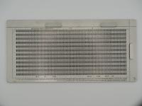
The board itself features a heavy, gold-plated proprietary edge connector on the bottom, marked with a barcode 02251906, the letters S.E.T., and serial strings 5604569B7731YH and C00556572. Flipping the artifact over reveals a mesmerizing, perfectly uniform ocean of thousands of through-hole solder joints.
Diving into the technical weeds, this board represents the pinnacle of mid-range mainframe packaging right before the total CMOS takeover. The central piece is a massive, custom IBM Ceramic PGA embedded onto a dense, multi-layer fiberglass PCB.
The gold lid is not just for visual prestige. In this era of bipolar gate arrays, thermal dissipation was a massive hurdle. Gold provided excellent thermal conductivity and extreme resistance to oxidation, pulling heat directly off the die and transferring it to ambient air or an attached heatsink.
The surrounding support chips tell a story of global supply chains. The JAPAN 6212451 chips are likely high-speed SRAM modules or custom glue logic fabricated overseas, while the CTS components are precision resistor networks used for signal termination across the heavy mainframe bus. The physical connectors and the absolute density of the through-hole pins indicate this board sat on a massive passive backplane, communicating with other specialized logic boards to form a complete computing system.
The late 1980s was an incredibly turbulent time for "Big Blue." They were fighting a brutal war on two fronts. Down below, cheap microcomputers were rapidly eroding their lower-end market share. Up above, aggressive supercomputer firms and rival mainframe clones were attacking their highly profitable enterprise sector.
IBM's response was to stretch their legendary System/370 architecture across every possible price point. While flagship machines utilized massive, liquid-cooled Thermal Conduction Modules, their mid-range systems had to rely on these dense, air-cooled logic boards.
There is a common myth that all vintage IBM mainframes ran incredibly hot and required sub-floor water cooling. Boards like this prove otherwise. They represent the transition era where heavy metal computing was slowly being miniaturized, forcing engineers to cram an unprecedented amount of logic onto single ceramic substrates while still relying on ambient air for survival.
Nailing down the exact machine that housed part number 74X1156 requires reading the tea leaves left by the date codes. The stamped numbers 8706, 8712, and 8731 on the support chips lock this board's manufacturing date squarely in the middle to late months of 1987.
The "IBM 34" etched on the gold lid is a classic red herring. While it is tempting to associate it with the IBM System/34, that machine was released in 1977 and discontinued in 1984. Instead, "34" is almost certainly a plant code or an internal fabrication designation used by IBM's microelectronics division.
Given the 1987 date codes and the form factor, I am placing this board in the IBM 9370 or late IBM 4381 family. The 9370, often called the "Baby 370," was released in late 1986 and heavily utilized these exact types of dense, single-chip ceramic modules surrounded by high-speed SRAM and logic to handle I/O and memory management. While I cannot confirm with absolute certainty if this specific board is the main ALU slice or a dedicated channel controller, the visual evidence and part taxonomy strongly point to it being a critical logic component of a mid-range late-80s IBM mainframe.