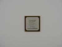
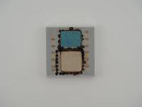
At first glance, you might mistake it for an early Athlon or Duron, but this is actually the central nervous system of a dual-processor server board. This specific unit features a dark, rigid organic pin grid array substrate, topped with a very distinct, stepped and stamped metal integrated heat spreader.
When observing the surface under good lighting, the contrast of the laser etching on the aluminum heat spreader is remarkably sharp. Even with the minor surface wear and a few specks of environmental dust, the transcription is effortless:
AMD™
AMD-762™
AMD-762JLC
B 0220DPAW A
© AMD 2000
ASSEMBLED IN
MALAYSIA
Additionally, printed directly onto the dark substrate in the bottom left corner is a faint identification mark: K 26949.
Flipping this artifact over reveals a dense, beautiful sea of 492 gold-plated pins. The brazing is immaculate, and the array is perfectly uniform, designed to drop cleanly into a high-density motherboard socket.
To appreciate this silicon, we have to look past the fact that it is not a CPU. The AMD-762 is a System Controller, universally known as a Northbridge, and it was the absolute anchor of the AMD 760 MP chipset. This chip handled the critical routing between two Athlon MP processors, the system memory, and the AGP graphics card.
The engineering brilliance here lies in the EV6 bus protocol, a technology AMD wisely licensed from Digital Equipment Corporation. Unlike Intel's shared front-side bus architecture of the era, which forced multiple CPUs to compete for the same data lane, the AMD-762 provided a dedicated point-to-point connection for each installed processor. This meant two Athlon MP chips could communicate with this Northbridge simultaneously without stepping on each other's toes.
Furthermore, this chip was a massive champion for DDR SDRAM. While the competition was trying to force the industry into adopting the notoriously expensive and hot-running Rambus RDRAM, the AMD-762 managed up to 4GB of PC2100 DDR memory, offering massive bandwidth with standard, affordable enterprise memory modules.
The historical prestige of this chip cannot be overstated. Before the AMD 760 MP chipset arrived, Intel maintained a near-absolute monopoly on the x86 dual-processor server and workstation market with their Xeon line. AMD was seen strictly as a budget desktop alternative. The release of the AMD-762 changed the entire landscape overnight.
The legend goes that Intel engineers were completely blindsided by the performance of dual Athlon MP rigs running on this exact chipset. The combination of the point-to-point EV6 bus and DDR memory allowed AMD to absolutely crush equivalent Intel systems in floating-point operations and memory bandwidth. It was the moment AMD proved they could build reliable, high-margin, enterprise-grade hardware.
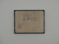
A common myth among amateur collectors is that any large pin-grid chip from this era is a processor. I frequently see these mislabeled in surplus bins as generic CPUs. But true hardware enthusiasts know that this piece of routing silicon is the literal grandfather to the massive I/O dies we see inside modern AMD Epyc processors today.
The prominent AMD-762 silkscreen on the heat spreader instantly classifies it as the primary system controller for the Socket A dual-processor platform.
Breaking down the surface codes gives us a perfect timeline for this artifact. The date code 0220 located on the third line of text indicates that this specific piece of silicon was packaged and finalized during the 20th week of 2002. The copyright year 2000 reflects the era the silicon design was locked in, right before the official 2001 launch of the platform. The JLC suffix on the part number typically denotes the specific revision and thermal rating for the packaging. This unit was likely pulled from an early 2000s workstation, perhaps an old Tyan Tiger or Asus dual-socket board, before finding its way into my permanent archive.