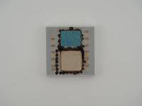
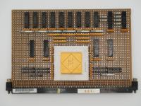
Holding this piece in my hand, the pure density of the white ceramic substrate is immediately striking. Weighing exactly 11.9g on my digital scale, this artifact feels like a solid tile of computing history. When I look through the 45mm Elmarit macro lens on my Olympus E-P7, the micro-contrast reveals incredibly fine details. The flip-chip die in the center has a beautiful teal and blue sheen, securely bonded by a thick, dark epoxy underfill.
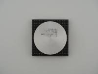
Looking closely at the laser-etched surface text, we can document the exact markings:
47P2532   9314   J190004H   1
260040-03
CORONADO 2.0
The date code 9314 firmly places the manufacturing of this specific unit in the 14th week of 1993. The ceramic is immaculate, lacking the typical thermal paste residue or mounting wear seen on pulled server parts, suggesting it might be a new-old-stock spare. The aesthetic cool factor is definitely present. While it lacks the massive gold lids of the older mainframe modules I usually hunt down, the exposed silicon die tells a compelling story of hardware miniaturization.
This artifact showcases IBM utilizing their highly advanced C4 packaging, also known as Controlled Collapse Chip Connection. In 1993, mounting a bare die face-down onto a ceramic substrate using microscopic solder bumps was a highly sophisticated fabrication process. This CBGA package allowed for a massive number of electrical connections compared to traditional wire bonding techniques.
The thermal challenges for chips of this era were actively shifting. Instead of sinking heat through a ceramic cavity and a brazed lid, the bare die here was designed to make direct contact with a thermal interface material and a heatsink. The intricate routing of traces, visible faintly beneath the surface of the ceramic, indicates a highly complex logic structure. This is a specialized IC built to handle heavy data traffic within a robust system architecture.
IBM loved giving their custom silicon majestic codenames, and Coronado 2.0 is no exception. During the early 1990s, IBM was heavily involved in expanding their mid-range server lines. These massive machines required an army of support chips to function. Chips like Coronado were the unsung heroes of the data center, acting as proprietary bus controllers or memory bridges to keep the main compute cores fed with data.
There is a funny hardware myth among some online scrappers who list these as highly valuable "antique CPU history witnesses" simply because they have IBM stamped onto the ceramic. In reality, they are bespoke ASICs. Securing this specific unit for the collection was a test of patience. The logistics of routing rare European finds through freight forwarders like Mailboxde often takes more effort than organizing a massive club tea session for my colleagues. Yet, adding a mysterious piece like Coronado to the archive makes the hunt entirely worth it.
While the 47P part number format is a dead giveaway for IBM logic components, unearthing the exact datasheet for a 1993 custom ASIC is virtually impossible. I am approaching this identification as an educated guess. The physical clues are undeniable. The font style, the part number structure, and the signature C4 packaging are exclusively IBM.
Based on the 1993 date code and the Coronado naming convention, my research points toward this being a specialized logic controller for a mid-range server system. It is very likely a bridge or controller for the POWER architecture systems of that specific era. The exact pinout and architectural block diagram remain unconfirmed. However, that lingering mystery is exactly why this artifact commands a permanent place in my museum. It represents the vast, undocumented ocean of custom silicon that quietly powered the corporate world in the 1990s.