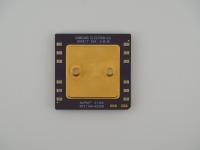
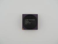
Holding this specific unit in my hand, the first thing that strikes me is the sheer, uncompromising density of it. Tipping the scales at exactly 46.7 grams, this is not your average consumer silicon. This artifact features a massive, perfectly circular aluminum heatsink bonded directly to the top of the ceramic substrate.
Looking closely at the crown of the heatsink, the laser-etched text is crisp and authoritative:
MITSUBISHI
M65201-0001WG
C2100
BWP2 100-3385 02
T JAPAN
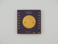
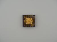
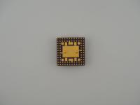
The physical textures of this chip are incredible. The dark ceramic package is industrial and cold, contrasting sharply with the bright, machined aluminum of the integrated cooler. The heatsink features distinct, deep concentric fins designed for aggressive airflow in a server chassis. Flipping the artifact over reveals a dense grid of gold-plated pins. I immediately noticed several bent pins and some accumulated fibrous debris along the outer edges, indicating this chip lived a long, hard life in a production environment before it was pulled. The center of the underside houses a dark, square thermal slug covering the die cavity, a hallmark of high-power continuous operation.
This piece is a textbook example of turn-of-the-millennium custom enterprise engineering. The M65201 designation points squarely to a high-density CMOS gate array or a highly customized Application-Specific Integrated Circuit (ASIC). During this era, off-the-shelf processors simply could not handle the massive, parallel I/O demands of enterprise storage arrays and core telecom switches.
To solve this, companies turned to fabricators like Mitsubishi to print custom logic architectures. The engineering challenge here was thermal density. Squeezing millions of logic gates into a single die meant the silicon generated intense, localized heat. The solution was brute force. They bonded a thick, metallic slug to the bottom and a massive, finned aluminum hat to the top. The Ceramic Pin Grid Array (CPGA) package itself is highly resistant to thermal expansion, ensuring that the hundreds of gold pins remain perfectly seated in their socket even as the chip rapidly cycles from room temperature to extreme operating heat.
Chips like this represent the "dark matter" of the computing world. They are the unsung, heavy-metal heroes that quietly powered the global infrastructure while the consumer market was entirely distracted by the Megahertz Myth and the desktop processor wars. There is a specific kind of romance to these custom enterprise ASICs. They were never advertised in magazines. They never had fancy marketing names. They were simply massive blocks of logic, built to run 24/7 in freezing, deafening data centers.
A common myth among casual collectors is that anything with this many pins and a built-in heatsink must be a supercomputer CPU. In reality, dedicated I/O controllers and memory crossbar switches often required significantly larger pin counts than the actual central processors of their time. They had to talk to dozens of memory banks and network interfaces simultaneously.
When I acquired this piece, the identity was shrouded in corporate obscurity. I do not have absolute, confirmed factory documentation for the M65201-0001WG, but I can confidently trace its lineage through the secondary part numbers.
The string 100-3385 02 is the golden clue here. This specific numbering convention is the signature of EMC Corporation, a titan of enterprise storage systems like the Symmetrix series. EMC heavily relied on custom silicon to manage their massive disk arrays and cache hierarchies. The BWP2 likely refers to a specific board or stepping within that storage architecture. The C2100 is almost certainly a date code pointing to the late 1990s or early 2000s, aligning perfectly with the physical construction methods. I am highly confident this artifact is a dedicated storage controller or cache management ASIC pulled from a decommissioned EMC SAN unit, representing a beautiful era when storage hardware required just as much heavy iron as the servers themselves.