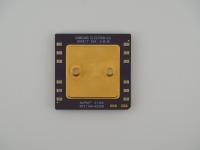
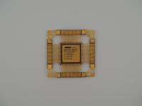
When I first picked up this artifact, the sheer density immediately stood out. Dropping it on the scale reveals a hefty weight of 38.6 grams, which is exceptionally chunky for a chip that measures only about 42mm by 42mm. The aesthetic is pure, unadulterated high-end enterprise hardware. We are looking at a brilliant white ceramic substrate topped with a massive, heavily machined metallic heatspreader.
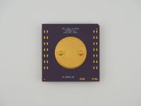
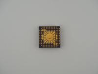
Flipping it over reveals an absolutely beautiful, high-density gold CLGA (Ceramic Land Grid Array). If you count the edges, it is roughly a 39 by 39 grid, yielding over 1,500 individual gold contact pads. The array is perfectly uniform except for a few missing pads at the very corners to key the orientation. The surface markings are laser-etched directly into the metal cap:
(hp invent logo)
3AC4-0004
41E4765
H17B00M0
(Data Matrix code)
Holding this piece, the cold metal and the flawless grid of gold on the back tell a story of extreme thermal dissipation and massive electrical I/O requirements. There are no bent pins to worry about here, just flat gold contacts designed to be clamped down under immense pressure into a server board socket.
To understand what this chip does, we have to talk about how HP built their massive, refrigerator-sized UNIX servers. This is not a traditional CPU. This is the sx2000 Cell Controller ASIC.
In high-end machines like the HP Integrity rx8640 or the legendary Superdome, the system is divided into "Cell Boards". Each cell board is basically an entire server unto itself, housing up to four Intel Itanium 2 processors (or dual-core PA-8900s) and massive banks of DDR2 memory. But those components cannot just talk to each other directly without a traffic cop. That is exactly what this ASIC does.
Sitting in the physical center of the cell board, the cell controller manages cache coherency, routes memory traffic, and provides the ultra-high-bandwidth links out to the system's central crossbar backplane. The reason it requires over 1,500 pads on the bottom is strictly due to bandwidth. It needs hundreds of traces dedicated to the memory bus, hundreds more for the processor front-side bus, and even more to link out to the external crossbar. It is an absolute monster of an integrated circuit.
I have to admit, there is a hilarious amount of misinformation floating around the internet about this specific chip. If you search for the part number 3AC4-0004, you will find hardware scavengers and surplus recyclers aggressively listing this as an "HP PA-RISC 7200 CPU" or an "Itanium rx8640 Processor".
This drives me absolutely crazy. The myth happens because recyclers rip these huge cell boards out of decommissioned Superdome chassis. They see a massive, socketed, ceramic chip sitting right next to the actual CPUs under a massive heatsink. Because it looks like a CPU, they assume it is a CPU. But the processors in the rx8640 were Intel Itaniums, which carried Intel branding. This chip proudly wears the "hp invent" logo because it is HP's proprietary silicon glue that made their entire server ecosystem function. It is the unsung hero of the enterprise data center.
I had to dig deep into my own archives and hardware datasheets to fully untangle the exact origin of this artifact. The "hp invent" logo immediately establishes a timeline between 1999 and roughly 2010.
The part number 3AC4-0004 is an internal tracking code used by Avago Technologies. When HP spun off their semiconductor and testing divisions into Agilent, and Agilent subsequently spun off its semiconductor products into Avago, Avago continued to fabricate these massive custom ASICs for HP's Enterprise division.
Interestingly, the second line of text (41E4765) looks incredibly suspicious. That specific seven-character alphanumeric format is famously used by IBM Microelectronics. During the early 2000s, IBM operated a massive foundry business manufacturing high-end ASICs for competitors. While unconfirmed without decapping the silicon to look for a foundry logo, it is highly plausible that Avago designed the logic and outsourced the physical silicon fabrication to IBM.
Regardless of which fab baked the wafer, visual clues completely prove its identity. The massive pad count, the lack of an instruction set branding, and the direct link to the rx8640 cell boards confirm this is a top-tier networking and memory controller ASIC. It is a fantastic piece of Cold-Room history.