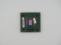
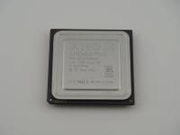
Holding this piece, I am immediately struck by the dense, premium weight of the ceramic substrate. Dropping it on the scale reveals it clocks in at exactly 27.7 grams. This specific unit features a gorgeous deep purple hue on the top package that is highly characteristic of late 90s fabrication plants. It feels rugged and industrial. The silkscreen text is stark white and perfectly preserved.
Here is the exact transcription of the surface text:
(Stylized N Logo) Geode™
GXLV- 200P 2.2V 85C
30046-23
© (M) 1995 - 1999 NSC
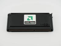
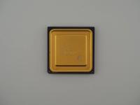
When looking at the back of this board, you are greeted by a brilliant staggered array of gold-plated pins. The brazing is immaculate and typical of high-quality late-century packaging. In the center sits a dark, slightly raised metallic or ceramic heat spreader plate. Looking through my macro lens, there is a very faint laser-etched code reading V5SK6030AF on that dark central square, and you can even see a faint fingerprint smudge left behind by whoever handled this artifact last. It is a beautiful, raw piece of computing history.
The National Semiconductor Geode is a fascinating piece of silicon because it is essentially a System-on-Chip from an era before the SoC concept was truly mainstream. Before we had modern APUs integrating everything onto a single die, the engineers behind this architecture decided to cram an x86 processor core, a memory controller, a PCI bridge, and basic graphics into a highly integrated package.
The surface markings tell us exactly how this chip operated. The 2.2V indicates the fairly low core voltage required to keep this 200 MHz part stable in cramped environments. It runs efficiently enough to max out at an 85 degrees Celsius thermal limit. The physical package is an SPGA-320 form factor. While it looks mechanically identical to a standard Socket 7 layout, electrically it is a highly customized beast designed for dedicated embedded motherboards and thin clients. You could not just drop this into a standard desktop board and expect it to post.
To truly appreciate the Geode, you have to look at the spectacular rise and fall of Cyrix. Cyrix originally designed this exact architecture under the name MediaGX. It was an ambitious attempt to conquer the extreme budget PC market by eliminating the need for expensive, separate motherboard chipsets. The concept was absolutely brilliant, but the execution was severely underpowered for heavy desktop use and struggled against Intel's sheer brute force.
Enter National Semiconductor. They swooped in, bought Cyrix in 1997, stripped out the desktop ambitions, and rebranded the highly integrated MediaGX core as the Geode in 1999. They pivoted the entire architecture away from traditional PCs and aimed it squarely at set-top boxes, thin clients, and industrial embedded systems. In that specific niche, it was a massive success. The irony of the Geode is that AMD would eventually purchase this division from National Semiconductor years later, bringing the rogue Cyrix DNA full circle back into the mainstream x86 rivalry.
This artifact leaves no room for ambiguity. The bold "NSC" copyright firmly dates this to the National Semiconductor era of the architecture, representing the exact moment after the Cyrix buyout was finalized and rebranded. The "200P" designation clearly flags it as a 200 MHz part, and the 1995-1999 copyright range aligns perfectly with the transition of the MediaGX IP into the Geode family.
I spent some time digging through old technical databooks to trace the V5SK6030AF etching on the back heat spreader. While standard National Semiconductor consumer documentation does not explicitly list this string, the alphanumeric format is a classic backend assembly lot code utilized by their Asian fabrication partners for internal tracking. There is no mystery here, just a perfectly preserved, beautifully heavy piece of early SoC engineering that helped bridge the gap between desktop processors and modern integrated circuits.