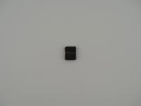
A chip that is far more mundane than the heavy iron I usually feature here, yet it possesses a stark, utilitarian cleanliness. This artifact lacks the heavy ceramic substrates and brazed gold pins of a true mainframe module. Instead, we have a classic black plastic Dual In-line Package.
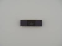
Top Marking:EPSON M80A87PB
(C) SEIKO EPSON CORP. 1994
LH53870C 9645 D
Bottom Marking:40
JAPAN
4
The top surface has a slightly matte, textured finish that diffuses light perfectly, allowing the crisp laser etching to stand out. The typography is completely unpretentious. Flipping the chip over reveals the injection molding artifacts and the stamped "JAPAN" origin mark nested between the 40 tinned pins. The pins themselves show very little oxidation, suggesting this unit was either socketed in a very clean environment or pulled directly from new-old-stock tubes.
At first glance, the "87" in the top part number might make a hopeful collector think of an Intel 8087 math coprocessor. However, the true nature of this silicon is exposed by the bottom line: LH53870C. This is a CMOS Mask ROM fabricated by Sharp.
Unlike EPROMs with their beautiful quartz windows or modern flash memory, a Mask ROM has its data physically baked into the silicon during the manufacturing process. The final metallization layer (the "mask") connects the internal transistor arrays to represent the specific ones and zeros of the compiled code. It is an incredibly cost-effective way to mass-produce firmware, but it means the chip is completely immutable. If Epson found a bug in the code after manufacturing, millions of these chips would become instant e-waste. The fabrication node is likely a highly mature 1.0 or 0.8-micron process, optimized purely for high yield and low cost rather than blistering speed.
This specific unit is not going to win any speed records or process complex floating-point math for a supercomputer. It is the definition of a blue-collar integrated circuit. Stamped with a 1994 copyright and a late 1996 production date code (45th week of 1996), this chip lived during the absolute golden age of bespoke peripheral hardware.
Seiko Epson was dominating the dot-matrix and early inkjet printer markets during this era. Lore dictates that chips exactly like this one held the complex firmware, proprietary font libraries, and carriage control logic for massive commercial printers or point-of-sale terminal systems. Without the silent work of Mask ROMs feeding perfectly timed instructions to microcontrollers, the business world of the 1990s would have ground to a halt. It is a humble piece of silicon, but an absolutely vital one.
Identifying this artifact required looking past the primary branding. The "EPSON M80A87PB" marking is an internal Epson software or firmware version code. Companies like Epson rarely spun up their own fabs for simple ROMs. Instead, they contracted out the physical manufacturing.
The giveaway is the LH53 prefix on the bottom row. This prefix is the universal identifier for Sharp's line of Mask ROMs. Sharp was a massive silicon foundry in the 1980s and 1990s, churning out memory for Nintendo cartridges, Apple logic boards, and countless consumer electronics. The "870" portion of the part number typically denotes an 8-Megabit capacity within Sharp's naming convention, which translates to exactly 1 Megabyte of dense, unchangeable code. While I cannot pinpoint the exact Epson printer or terminal this was destined for without dumping the ROM and reverse-engineering the hex code, the physical evidence overwhelmingly proves it is a dedicated memory module acting as the digital brain for mid-90s office hardware.