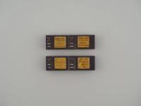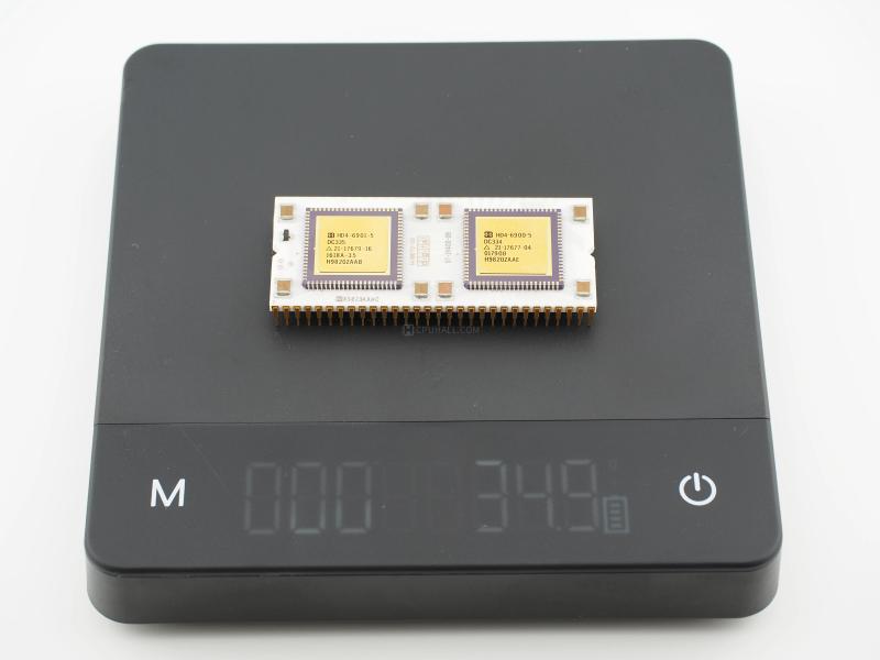
This artifact is a masterclass in 1980s high-end logic packaging. The substrate is a pristine, heavyweight white ceramic, serving as the foundation for two deeply recessed silicon dies. Each die is protected by a brilliant gold-plated cap, surrounded by a dark purple ceramic framing that provides a gorgeous visual contrast.
Here is the exact transcription of the surface text:
Left Chip:[Logo] HD4-6901-5
DC335
[Triangle] 21-17679-16
1618A-3.5
H9820ZAAB
Right Chip:[Logo] HD4-6900-5
DC334
[Triangle] 21-17677-04
01790B
H9820ZAAE
Center Substrate:1418673-00
[digital logo in blocks]
57-19400-09
Bottom Edge:[Fab Mark] X9823AAAC
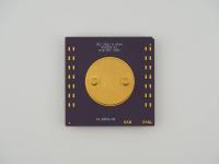
Flipping this artifact over reveals the faint internal routing traces shadowed beneath the white ceramic surface. The pins are thick, gold-plated, and beautifully side-brazed along the long edges of the package. It is heavy, cold to the touch, and feels like a piece of military-grade hardware. The tiny surface-mount passive components flanked around the chips on the top side indicate strict power delivery requirements right at the silicon level.
This module represents a fascinating pinnacle of computer architecture: the miniaturization of a refrigerator-sized minicomputer onto a single ceramic block. Code-named "Jaws" during its development, the J-11 architecture was an ambitious project to condense the entire performance and feature set of the legendary PDP-11/70 into a microprocessor format.
To achieve this, DEC partnered with Harris Semiconductor to utilize their advanced CMOS fabrication process. The processing duties were split across two distinct dies mounted on the shared ceramic substrate, keeping signal latency exceptionally low:
The -09 suffix on the substrate part number (57-19400-09) specifically identifies this as the 18 MHz variant of the DCJ11-AE.
While DEC's VAX architecture often dominates discussions of minicomputer history, it was the PDP-11 that truly changed the world. The PDP-11's highly orthogonal instruction set directly influenced the design of the C programming language, and by extension, the creation of the UNIX operating system. Every modern system owes a structural debt to the PDP-11.
The J-11 module was the ultimate evolution of this architecture. It allowed systems builders to drop the computing power of a massive 1970s mainframe directly into embedded systems, ruggedized military gear, and high-end workstations. It is a physical reminder of a time when computer companies designed their own instruction sets from scratch and engineered custom packaging meant to survive an apocalypse.
While the J-11 was introduced in 1983, the most fascinating detail of this specific artifact lies in its date codes. The H9820 and X9823 codes indicate a manufacturing run in the 20th and 23rd weeks of 1998.
This is an extraordinarily late date for a PDP-11 processor. By 1998, DEC's Alpha architecture had already peaked, and the company was being acquired by Compaq. The existence of a newly minted J-11 in 1998 strongly suggests this module was manufactured as a high-reliability, high-cost replacement part for legacy industrial, military, or telecommunications infrastructure. Many mission-critical systems built in the 1980s simply could not be upgraded, and companies paid a premium to keep their PDP-11 hardware alive well into the 21st century.
A piece with this kind of historical weight and late-stage provenance is a perfect candidate for long-term archiving in a ~40% relative humidity dry cabinet, ensuring the side-brazed pins and pristine ceramic remain untouched by oxidation for decades to come.