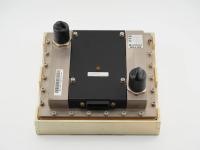
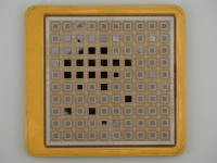
When I unlatched the original brown plastic DEC clamshell case, I knew I was looking at something special. The texture of the gold substrate and the delicate, transparent orange polyimide flex ribbons around the perimeter practically glow under studio lighting.
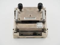
At first glance, the massive array of gold-plated pins on the bottom looks like a colossal CPU socket interface. However, looking closely at the heavy Torx screws embedded directly in the pin field, it becomes incredibly obvious that these are not electrical contacts. They are thermal transfer pins for an extreme air-cooling plenum. The actual electrical connections are those four fragile, high-density flex cables wrapped around the edges.
Center Substrate Marks:digital (Logo)
ALL RIGHTS RESERVED (C) 1989
5018683-01 B2-2-
MUI P1003
Sticker:+V212001-06+
Gate Arrays:M (Logo) SC63911 TA02 UUAG C00D5 144A0
M (Logo) SC55001 TA64 UUAE C0642 138B0
M (Logo) SC55001 TA65 UUAN C0652 136D0
UUBT C00A5 11610 (Center)
Housing & Date Codes:70-27930-01 REV B01 RMC 22/91
MMS 12-33595-01
70-27213-01 REV D04 RMC 18/91
74-39133-01 REV D3 RMC 20/91
Barcode Tape:*V212001.6*
*H02*
*CT15001004*
*P1003-AA*
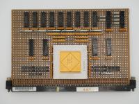
This is heavy metal engineering from the absolute peak of the ECL (Emitter-Coupled Logic) era. The VAX 9000 logic is based on the Motorola MCAIII emitter-coupled-logic gate array technology. These specific gate arrays were fabricated in Motorola's MOSAIC III bipolar process, which featured a drawn width of 1.75 micrometers and three layers of interconnect. A fully built VAX 9000 CPU required 13 of these MCUs (Multi-Chip Units) working in tandem, operating at a 62.5 MHz clock speed with a 16 ns cycle time.
The packaging is arguably more impressive than the silicon itself. DEC developed a High Density Signal Carrier (HDSC) to mount these chips. This substrate is a deposited thin-film structure consisting of nine metal layers of extremely fine-line copper and polyimide. Because standard pins could not handle the necessary signal density, the data pathways exit the module through those four flexible circuit interconnect assemblies. Each flex connector packs 268 contacts into a footprint of just two square inches. The raised contact bumps on the flex circuits are solid copper plated with nickel and gold. A fully populated 9000 CPU board featured over 16,000 of these separable interconnects.
Thermal management was a nightmare. Initially, DEC designed the system to require IBM-style water cooling to hit performance targets, which they codenamed Aquarius. Eventually, their thermal engineers developed a highly advanced air-cooling system to replace the water loops, resulting in the Aridus models. The massive gold pin-fin array on the bottom of this artifact is the Aridus air-cooled heat sink.
The VAX 9000 was meant to be DEC's ultimate "IBM killer", designed to deliver unmatched mainframe performance at a much lower price point. The company poured an estimated $1 billion into the research and development of this architecture. It was a monumental gamble.
One of the most fascinating pieces of lore surrounding this hardware is how it was actually designed. DEC utilized an artificial intelligence expert system called SID (Synthesis of Integral Design) to generate the logic gates. SID took high-level behavioral sources and synthesized approximately 93 percent of the scalar and vector units. The AI was so capable that it could balance conflicting rules for speed, physical size, and wiring loads better than a team of expert human logic designers.
Unfortunately, the real world is brutal. By the time DEC finally solved their production issues and got the machine to market, the microcomputer revolution had already caught up. Newer, vastly cheaper RISC processors and DEC's own NVAX chips were offering a huge fraction of the 9000's performance for practically nothing. The VAX 9000 was a massive commercial failure, with roughly four dozen systems delivered before production was killed entirely.
There is absolutely no ambiguity about the identity of this hardware. The visual clues are ironclad. The combination of the DEC 1989 copyright on the center HDSC, the specific Motorola MCA III gate arrays, and the tell-tale orange flex-circuit interconnects perfectly matches the engineering documentation for the VAX 9000 packaging.
Furthermore, the physical construction proves this is an Aridus air-cooled variant. The water-cooled Aquarius MCUs had screw-in liquid coolant connectors on the back. The dense bed of thermal pins on this unit confirms it was designed to be mounted to a massive air column plenum. Reading the date codes etched into the aluminum housing (18/91, 20/91, 22/91), we can see this specific piece was manufactured in mid-1991. This aligns perfectly with the extremely narrow window where the VAX 9000 was actually shipping before the entire mainframe project was permanently shelved.