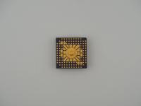
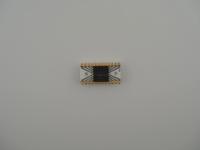
Holding this piece is like holding a brick of concentrated engineering. The sheer mass of the aluminum heat spreader attached to the dense ceramic substrate is staggering. Getting this heavy artifact properly lit for the camera was a chore, but the lens beautifully exposes the flawless gold contact grid on the underside.
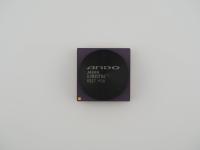
Here is the exact surface transcription from the metal cap:
cadence (R)
41M8337  PQ
2000000006979
IBM93 0003MGF000
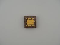
On the side of the white ceramic substrate, we can see the laser etched batch codes:
07BM01579
+ 07BM01579 (inverted)
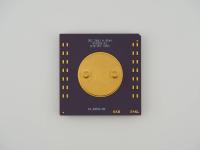
The contrast between the industrial aluminum top and the stark white ceramic bottom is pure vintage high-end computing aesthetic. Peeking around the edges of the heat spreader, a thick, dark grey epoxy seal ring is visible. This structural bond is the only external hint that this is not a single piece of silicon, but a highly complex Multi-Chip Module (MCM) hidden beneath the metal. The massive Land Grid Array on the bottom is incredibly dense, designed to feed power and parallel I/O to a multitude of components simultaneously.
Internally, this artifact abandons standard single-die processing for a heavily populated multi-chip architecture. Hidden beneath the aluminum lid are two large, flip-chip logic dies built on IBM’s 90nm process. These dies house a combined 1,536 custom boolean logic processors.
Unlike a standard CPU or traditional FPGA, these processors are purpose-built to accelerate hardware emulation, taking compiled netlists of unreleased silicon and solving massive boolean equations simultaneously. Flanking these logic dies are eight Hynix GDDR memory chips, providing 128MB of high-speed local memory.
IBM Microelectronics leveraged their mastery of high-density ceramic packaging to make this possible. The massive white ceramic substrate is a complex, multi-layered alumina matrix. It takes the microscopic signals from the C4 micro-bumps of the logic dies and the BGA connections of the memory chips, fanning them out flawlessly to the expansive LGA grid underneath without bottlenecking the intense data throughput required for emulation.
The EDA hardware market is a fascinating, secretive world. Systems like the Cadence Palladium II are sold by the rack, sitting in highly secured server rooms to verify the designs of future industry-defining microprocessors.
Because these emulation clusters could cost millions of dollars, it is incredibly rare to see individual MCMs escape into the wild. Typically, proprietary hardware of this caliber is securely destroyed upon decommissioning to protect intellectual property. A common misconception in vintage hardware preservation is that these thick, heavy IBM93 packages contain standard ASIC silicon. In reality, the shift to custom, densely packed MCMs allowed Cadence to drastically increase compilation speeds and simulation capacity over single-die predecessors, cementing the Palladium II as legendary heavy iron among verification engineers.
Identifying this precise configuration relies on matching physical packaging dimensions with historical teardowns. While the cadence and IBM93 markings establish the foundational provenance, the true identity lies in the physical scale.
The aluminum lid spans approximately 82mm, leaving a ceramic substrate width of about 75mm. This expansive footprint perfectly matches the spatial requirements for the dual-die, eight-memory-chip layout of the Palladium II node, definitively separating it from the physically smaller, single-die ET4 predecessor. The 41M8337 part number and side substrate markings confirm the IBM manufacturing origin from the mid-2000s. Correctly categorizing the architecture and hardware type of this artifact ensures its proper placement as a premier example of high-density IBM engineering.