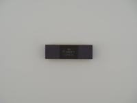
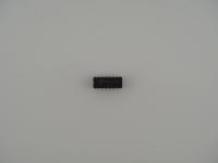
Here we have a stunning example of late 1970s semiconductor packaging, fabricated in early 1980. This specific unit is a ceramic Asynchronous Communications Interface Adapter, better known as an ACIA.
Before getting into the silicon, we have to appreciate the external packaging. Holding this piece under a macro lens reveals an incredible level of material contrast. The substrate is a brilliant, stark white ceramic, which feels dense and cold to the touch. Radiating outward from the central black cap are thick, exposed gold traces. They look almost like a sunburst, a beautiful aesthetic choice dictated entirely by the engineering requirements of a side-brazed package.
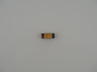
Here is the exact transcription of the surface text, read from the slightly faded stamping on the central black lid:
AMI 8020CB
S6850M
KOREA
Additionally, there is a distinct Z printed directly onto the white ceramic on the right-hand side. The most unusual physical trait of this specific artifact is the presence of two mounting holes bored entirely through the ceramic substrate. The side-brazed pins themselves show a rich, warm gold plating, indicating a package designed for high reliability and longevity rather than cheap commercial assembly.
This chip is not a central processing unit, but rather a vital piece of specialized silicon that made early computing practical. The 6850 is a UART (Universal Asynchronous Receiver/Transmitter) designed specifically for the 8-bit Motorola 6800 bus architecture.
In the late 1970s, moving data out of a parallel bus and into a serial format for teletypes, modems, or external terminals was a complex task. The S6850 handled the heavy lifting. It provided data formatting, error checking, and control interfacing. Built on NMOS technology, it required careful thermal management and precise clocking to ensure serial data integrity.
The CDIP-24 (Ceramic Dual In-line Package) used here is a marvel of retro-engineering. Side-brazed packages were significantly more expensive to produce than standard plastic or even glass-sealed cer-DIPs. The manufacturing process involved stacking layers of unfired ceramic tape (alumina) printed with refractory metal traces (usually tungsten). After firing the layers together at extreme temperatures, the external tungsten traces were plated with nickel and then pure gold. The pins were then brazed directly to the sides of the package. The central cavity housing the delicate silicon die was finally sealed with the black lid you see here, likely using a glass-frit seal to ensure a hermetic environment.
While Intel was pushing the 8080 and 8251 USART, Motorola was building an ecosystem around the 6800 family. The 6850 became the absolute gold standard for serial communications in the late 1970s and early 1980s.
It was the beating heart of countless early modem boards, S-100 bus serial cards, and industrial control systems. If a piece of early vintage computing hardware needed to talk to the outside world over a serial line, there is a very high probability a 6850 was coordinating the handshake.
A common myth is that all 6800-series peripherals were strictly locked into Motorola CPUs. In reality, the 6850 was incredibly versatile. Because of its straightforward bus interface, designers frequently paired it with the MOS Technology 6502.
There is also a funny irony in finding an American Microsystems Inc. (AMI) logo on a piece of Motorola architecture. In the wild west of the early semiconductor industry, second-sourcing was a requirement for military and massive industrial contracts. Buyers demanded a backup manufacturer in case the primary fab burned down or failed to meet yield. AMI made a fortune perfectly cloning and legally second-sourcing parts from the big players, often wrapping them in packaging that looked significantly more premium than the originals.
Identifying this artifact is highly straightforward due to the clear markings, but the exact suffix and physical anomalies require a deeper look.
The 8020 date code firmly places the manufacturing of this specific unit in the 20th week of 1980. The CB likely denotes the specific package and revision batch from the Korean assembly plant. The S in S6850 is AMI's standard prefix for their second-source logic, replacing Motorola's MC.
The M suffix at the end of S6850M is the critical clue to its premium build. In AMI nomenclature, an M suffix frequently denoted a wider temperature tolerance or a military-grade screening process. This perfectly explains the use of the expensive side-brazed white ceramic package instead of a standard plastic DIP.
The two through-holes in the ceramic substrate are highly unusual for standard consumer or server applications. Based on historical telecom and aerospace hardware, these holes were utilized for robust mechanical mounting. In environments subject to high vibration, such as avionics or heavy industrial machinery, relying solely on the solder joints of the pins was a failure risk. Screws or nylon standoffs would pass through these holes to physically anchor the heavy ceramic package directly to the PCB.