The Trojan Horse. The T2 was a custom ARM chip placed inside Intel Macs to handle security, encryption, and the Touch Bar. Ostensibly, it was there to make Macs more secure.
In reality, it was Apple testing their own silicon inside high-performance machines, gathering data and refining their drivers before kicking Intel out entirely. It is the bridge between the Intel era and the Apple Silicon era.
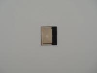
Apple heavily glues and solders these chips into their aluminum chassis, meaning you rarely get to see the raw silicon package out in the open.
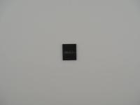
Turning the artifact over, the underside reveals a dense grid of BGA pads where the solder balls have been cleanly removed. The top side is where the real visual intrigue lies. We have a green organic substrate carrying not just the compute die, but the system memory. The main processor is covered by a flat, utilitarian silver heat spreader adorned with the iconic Apple logo. Right beside it sit two matte black memory packages.
Under the macro lens, the laser etching on the metal heat spreader becomes crystal clear:
U046T5Z1AL 2133
APL1102 339S00881E
The faint micro-contrast text on the adjacent black memory modules reads H9HCNNNCRMML, revealing them to be SK Hynix LPDDR4X DRAM packages. The 2133 date code on the main die indicates this piece was fabricated in the 33rd week of 2021. The physical texture is a stark contrast between the cold metal of the integrated heat spreader and the smooth epoxy of the memory chips.
This artifact represents a monumental shift in consumer computing engineering. Fabricated on TSMC's cutting edge 5nm process node, the APL1102 packs a staggering 16 billion transistors.
The true engineering marvel here is the Unified Memory Architecture. By placing the SK Hynix DRAM directly onto the same organic package as the system-on-chip, Apple drastically reduced the physical distance data had to travel. This eliminated the traditional latency penalty of routing memory traces across a large motherboard. The CPU, GPU, and Neural Engine all share the exact same memory pool. They do not need to copy data back and forth between discrete RAM pools.
Internally, this chip utilizes a big.LITTLE core configuration. It features four high performance "Firestorm" cores running up to 3.2 GHz and four high efficiency "Icestorm" cores for background tasks. This aggressive wide-decode architecture allowed it to execute massive amounts of instructions per clock, entirely changing the thermal and acoustic expectations for personal computers.
The historical prestige of this chip cannot be overstated. For over a decade, the industry myth was that ARM architectures were strictly for phones and tablets. Power users believed ARM could never scale up to challenge x86 giants like Intel and AMD in the desktop space.
When Apple announced the M1, the broader hardware community was deeply skeptical. Then the benchmarks leaked. A fanless, entry level MacBook Air equipped with this exact chip was suddenly dismantling high end, actively cooled Intel Core i9 laptops in both single core performance and battery life. It was an absolute bloodbath.
This specific silicon marks the exact moment Apple initiated their two year transition away from Intel processors, a project internally rumored as Project Kalamata. It forced the entire PC industry to scramble and reevaluate their roadmaps. Seeing it sitting here bare, stripped of its pristine aluminum host, is a visceral reminder of the tectonic shift it caused.
Identifying this piece is highly straightforward due to Apple's consistent part numbering. The APL1102 designation is the definitive internal Apple part number for the original M1 chip.
The layout is the ultimate giveaway. Prior to this generation, Apple's A-series iPad and iPhone chips used Package-on-Package designs where the RAM was stacked vertically directly on top of the compute die. The M1 moved to this adjacent layout to accommodate the thermal requirements of a desktop class processor while still keeping the memory on the same substrate.
Because Apple does not sell their chips to third parties, raw units like this only exist in the wild if they are harvested. This specific processor was certainly desoldered from a dead MacBook or Mac Mini logic board, likely harvested by a repair shop in Shenzhen before making its way into the collection.