The Declaration of Independence. The A4 was the first processor designed in-house by Apple (using ARM architecture). It powered the original iPad and the iPhone 4. Before this, Apple relied on Samsung and PortalPlayer for their mobile brains.
By designing their own silicon, Apple could tailor the hardware exactly to iOS, achieving smoothness and battery life that Android competitors couldn't match with off-the-shelf parts. This chip marks the beginning of Apple's journey to become the most valuable company on Earth.
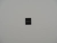
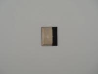
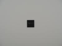
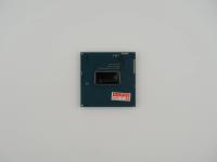
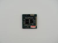
Holding this piece is a hilarious contrast to handling a heavy ceramic mainframe module. Here we have a textbook example of high-density mobile packaging. It is a deceptively simple black square of resin, yet it represents a seismic shift in computing history. Looking at the back of this board, the sheer density of the BGA (Ball Grid Array) solder pads is striking. The pads are arranged with a highly specific footprint, leaving a rectangular void in the very center.
When I angle the top surface against the light, the micro-contrast of the laser etching reveals a wealth of data scattered across the package.
APL0398 339S0151
[Apple Logo] A4
VTKEAG10QA 1236
H9DKNNN4HKAPTR-NEM
S13X9P6 1240
The texture of the black epoxy is smooth and completely utilitarian. There are no gold caps or brazed pins here. It is a mass-produced slab of modern mobile silicon, but the exact string of characters tells a brilliant story. The 1240 date code at the bottom right indicates this specific unit was packaged in the 40th week of 2012. This is fascinating because the A4 debuted in 2010. Finding a 2012 manufacturing date suggests this artifact was likely bound for a late-run 8GB iPhone 4 or a second-generation Apple TV.
This artifact is not actually a single chip. It is a PoP (Package on Package) assembly. The A4 System-on-Chip (SoC) sits at the base, directly interfacing with the BGA pads on the bottom. Stacked right on top of that logic die within the exact same package is the system RAM.
The vertical string on the right side H9DKNNN4HKAPTR-NEM is the giveaway. That is not an Apple part number. That is a strict SK Hynix component code for Mobile DDR SDRAM. By sandwiching the memory directly on top of the processor, the engineers drastically reduced the physical footprint on the motherboard and shortened the electrical traces to improve memory latency and power consumption.
At the silicon level, the APL0398 logic die was fabricated by Samsung on a 45-nanometer process. Inside, it houses a single-core ARM Cortex-A8 processor alongside a PowerVR SGX535 graphics core. While it ran at 1.0 GHz in the original iPad, it was slightly underclocked to 800 MHz for the iPhone 4 to manage thermal output and battery drain in a tighter chassis.
This specific architecture is the spark that ignited the entire modern Apple Silicon empire. Before the A4, mobile devices relied on off-the-shelf processor designs. The original iPhone and the 3GS used standard Samsung ARM chips. The A4 changed the rules of the game entirely.
Apple had quietly acquired P.A. Semi and Intrinsity, two legendary chip design firms with serious talent in low-power architecture. The resulting A4 was a massive flex. It was the heart of the original iPad and the retina-display iPhone 4.
A common myth is that the A4 was a 100% custom ground-up design by Apple. In reality, it was incredibly similar to the Samsung S5PC110 (also known as the Hummingbird). Apple and Samsung co-developed the core, utilizing Intrinsity's Fast14 technology to squeeze higher clock speeds out of the Cortex-A8 architecture without melting the phone. The A4 proved that controlling the silicon was the only way to build a truly optimized mobile device.
Identifying this artifact is an absolute certainty. The prominent Apple logo and the classic A4 branding are universally recognizable. Furthermore, the APL0398 part number at the very top is the definitive, documented Apple identifier for this specific generation of SoC.
My analysis of the physical traits confirms its exact configuration. The SK Hynix memory string proves this is the complete PoP assembly and not just a bare die. Examining the BGA pad layout on the underside matches perfectly with known mainboard schematics for devices of that era. The late 2012 date code makes this specific unit a fun anomaly for the collection, representing the tail-end production of a legendary architecture just as the industry was aggressively shifting toward multi-core designs like the subsequent A5.