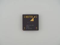
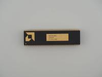
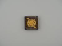
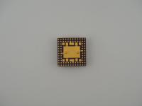
There is an undeniable gravity to vintage ceramic silicon, and this specific unit represents absolute peak aesthetic for early microprocessor packaging. Weighing in at exactly 15.5g on the scale, this is a substantial chunk of computing history. The first thing that strikes me when holding this piece is the striking contrast of the deep purple ceramic substrate against the brilliant gold cap and the matching gold trace extending toward the pin 1 indicator.
(M)
MC68000L10
GN78507
Every single one of those 64 pins is a testament to an era when chips were built like absolute tanks.
Diving into the silicon itself, the Motorola 68000 is an architectural masterpiece of its time. It features a 32-bit internal instruction set and register pool, paired with a 16-bit external data bus and a 24-bit address bus. While the name implies 68,000 transistors, the actual active transistor count on the die sits closer to 40,000, fabricated using advanced HMOS technology.
This specific artifact runs at a clockspeed of 10 MHz, which was a very respectable bump up from the original 8 MHz launch parts. The sheer size of this package, measuring roughly 3.2 inches long, was born out of pure engineering necessity. Motorola engineers made the bold decision to avoid the multiplexed address and data lines that Intel utilized on the 8086. By keeping the buses separate for better performance and easier programming, they required far more physical pins. The result is this massive 64-pin ceramic package that dominates any motherboard it sits on. The gold cap you see on top isn't just for show. It acts as an environmental seal and assists in managing the thermal load generated by the die sitting directly beneath it.
If you look at the foundation of the 1980s computing revolution, the m68k architecture is the bedrock. This is the silicon that powered the original Apple Macintosh, the Amiga 1000, the Atari ST, and early Sun Microsystems UNIX workstations. It even found a massive home in the arcade and console space, serving as the roaring heart of the Sega Mega Drive and Genesis.
The lore surrounding the 68000 usually centers on its beautiful, orthogonal instruction set. Programmers absolutely loved writing assembly for this chip compared to the segmented memory nightmare of contemporary x86 processors. It felt like a minicomputer architecture perfectly shrunk down onto a single microprocessor. There is a persistent myth that the 68000 was completely flawless from day one, but early steppings did have bugs regarding how interrupts were handled, which is why chips like the 68010 were eventually necessary to fully support virtual memory. Still, the 68000 remains one of the most culturally significant architectures ever etched into silicon.
Identifying this artifact is a straightforward joy due to Motorola's highly logical naming conventions of the era. The MC prefix confirms this is a fully qualified, commercial-grade component rather than an XC prototype or engineering sample. The 68000 is the core model. The L signifies the gorgeous ceramic side-brazed DIP package, while the 10 denotes the 10 MHz speed grade.
The third line of text, GN78507, is an internal Motorola batch or mask trace code. Collectors often try to read standard date codes into these strings, but early Motorola foundry markings frequently utilized custom lot formats. The 785 portion might tempt someone to guess a 1978 manufacturing date, but the 68000 architecture was only formally introduced in 1979. It is highly probable that GN78507 points to a specific fab run or mask revision from the early 1980s when the 10 MHz variants began rolling off the assembly line in higher volumes.