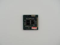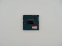
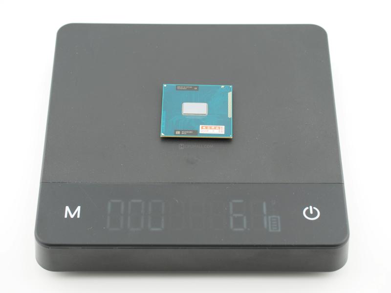
Holding this piece, I immediately noticed how incredibly light it is. Dropping it on the scale confirms it weighs exactly 6.1 grams. Flipping the chip over reveals a dense grid of gold-plated pins, confirming a Pin Grid Array design. Unlike desktop processors of the era, this chip was never meant to wear a metal Integrated Heat Spreader. It is natively a bare-die component designed to save vertical space inside a laptop chassis.
Looking closely at the edges of the central mirror-like silicon die, you can see a thick grey bead of underfill epoxy. This is factory applied to protect the microscopic C4 solder bumps connecting the die to the substrate from thermal expansion stress.
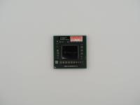
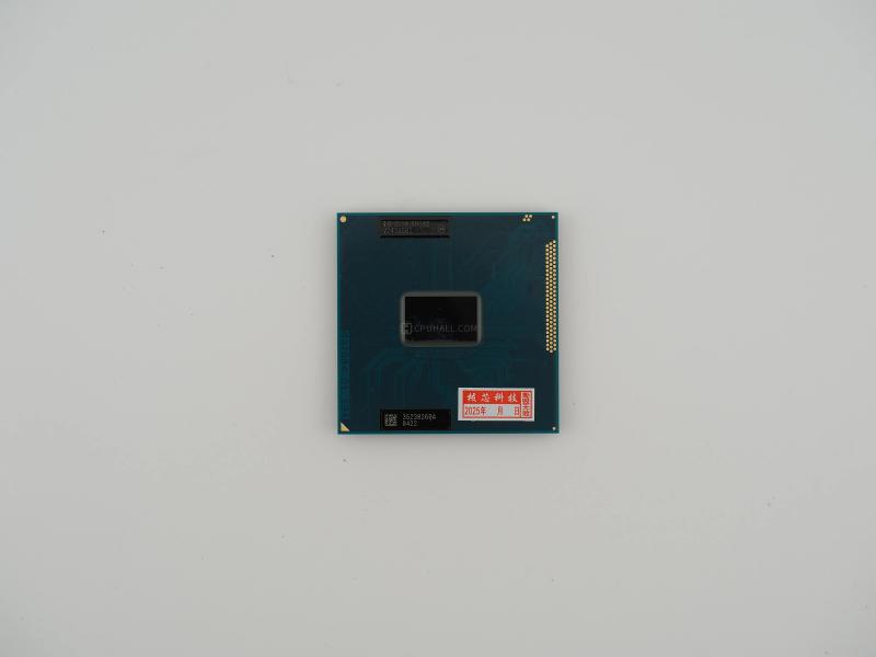
Flipping through the macroscopic details, the story gets even better. On the top edge of the green substrate, there is a tiny, laser-etched black label embedded in the PCB.
i (M) (C) 10 SR102
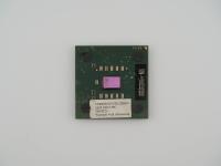
V243A582 (e4)
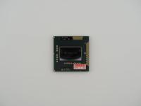
On the bottom edge, there is another microscopic data matrix sticker right next to the Intel substrate code.
35238260A
0422
Substrate Print:
G37084 01 S34
To top off the bizarre visual profile, the bottom right corner features a bright red, tamper-evident warranty sticker printed in Chinese. It reads "核芯科技" (Core Technology) with a warranty expiration date extending out to the year 2025. It is a beautiful clash of high-end Intel engineering and gray-market hardware recycling.
Beneath that exposed, shiny rectangle lies the heart of Intel's 3rd Generation Core architecture, codenamed Ivy Bridge. Fabricated on Intel's groundbreaking 22nm process utilizing 3D Tri-Gate transistors, this specific piece of silicon is a dual-core configuration without Hyper-Threading.
The die we are looking at is incredibly small and dense. Because it is a mobile budget chip, it runs exceptionally cool with a Thermal Design Power rating of just 35 watts. It handles both traditional processing and basic display output, housing Intel HD Graphics right on the same piece of silicon.
Flipping the chip over reveals the 988 gold contact pins of the Socket G2 interface. The central capacitor arrangement is incredibly sparse, perfectly matching the low power delivery requirements of a budget dual-core die rather than the heavily populated capacitor islands you see on the mobile i7 quad-core variants of the same generation.
This artifact tells a very specific, almost nostalgic story about the twilight of modular laptop hardware. The Socket G2 interface represents one of the final generations where a consumer could easily open up a budget notebook, turn a single flathead screw to unlock the CPU socket, and physically swap out the processor for an upgrade. Shortly after this era, Intel shifted almost entirely to BGA packaging for laptops, meaning the processor was permanently soldered to the motherboard.
This specific Celeron 1000M was the sacrificial chip of that era. Budget buyers would purchase the cheapest laptop possible that housed this Celeron, then immediately order a used Core i7 mobile processor online to swap into the socket for massive performance gains at a fraction of the retail price.
The "Core Technology" Chinese warranty sticker completely solidifies the modern provenance of this leftover chip. There is a massive secondary market on platforms like Taobao where older processors are stripped from e-waste, tested to ensure they still boot, slapped with a new warranty sticker, and sold in bulk. This specific chip was likely pulled from a dead office machine and thrown into a recycling tray, waiting to be purchased for single-digit dollars to revive another aging notebook.
Identifying this bare-die mobile chip was an exercise in reading the micro-text. The critical clue is the S-Spec etched into the top black label: SR102. Cross-referencing this code instantly points to the Intel Celeron 1000M.
The Batch Code or FPO (Finished Process Order) V243A582 confirms the manufacturing timeline. The "V" indicates the fabrication plant, the "2" stands for 2012, and the "43" means it rolled off the line in the 43rd week of that year. This perfectly aligns with the processor's official retail launch window in the first quarter of 2013. The (C) 10 copyright mark next to the Intel logo simply refers to the year 2010 when the package labeling standard or specific substrate layout was originally patented.
The presence of the native underfill epoxy and the physical gold pins immediately proved my previous assumption of this being a desktop LGA chip completely wrong. This was born and bred as a mobile powerhouse, or in this case, a mobile budget placeholder.