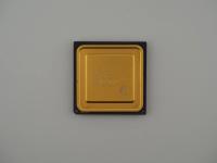
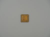
Registering at exactly 6.9 grams on the scale, this is a beautiful example of late-20th-century British semiconductor engineering.
The gold lid is brazed beautifully to the dark body, and the top-left corner features the iconic trace routing to indicate pin 1 alignment. Flipping the chip over, the 84 gold-plated pins are arranged in an 11x11 grid with a hollow center, and they remain remarkably straight and unoxidized.
Here is the exact transcription of the visible markings:
Front Gold Cap:Ⓜ INMOS ∆
IMST805-G25S
III CF 9318
Front Ceramic Base:M 9320 I
3110 U.K.
The Ⓜ is the standard mask work copyright symbol, followed by the manufacturer name. The G25S indicates a PGA package running at 25 MHz. The date codes on the cap (9318) and the ceramic (9320) place the assembly of this specific unit right around mid-1993, manufactured in the United Kingdom.
Diving into the technical weeds, the IMST805 is a 32-bit microprocessor that was radically different from anything Intel or Motorola was doing at the time. It is a Transputer. The fundamental concept here was to put an entire computer on a single chip to facilitate massive parallel processing.
The T805 specifically features a 32-bit integer CPU, an integrated 64-bit floating-point unit (FPU), 4KB of on-chip static RAM, and most crucially, four high-speed serial communication links. These links allowed Transputers to be daisy-chained together into massive arrays without the need for complex external bus arbitration logic. You could literally just wire the serial output of one Transputer to the input of another, and they would communicate autonomously.
Fabricated on a CMOS process, the chip ran efficiently enough that thermal management was rarely a critical issue compared to the bipolar monoliths of the mainframe world, hence the relatively simple ceramic PGA package without massive integrated heat spreaders. The integrated hardware scheduler was a stroke of genius, capable of context switching between parallel processes in less than a microsecond.
The lore of INMOS is essentially the story of the British government attempting to brute-force a domestic silicon valley. Backed heavily by state funding in the late 1970s and 1980s, INMOS designed the Transputer to be the building block of fifth-generation supercomputers.
The ambition was staggering. Instead of a single powerful CPU, the future was supposed to be thousands of cheap Transputers working in harmony. This architecture saw genuine use in academic supercomputers like the Meiko Computing Surface and various specialized embedded systems. However, the commercial triumph INMOS hoped for never materialized.
The downfall was largely software. To truly unlock the power of the Transputer, you had to program in occam, a concurrent programming language specifically designed for the chip. While brilliant, occam was alien to an industry rapidly standardizing on C and standard UNIX operating systems. By the time INMOS released robust C compilers, standard RISC processors and Intel's x86 juggernaut were accelerating so fast that a single conventional CPU could outpace a small cluster of Transputers. SGS-Thomson eventually acquired INMOS, and the standalone Transputer faded into the realm of beautiful esoteric hardware.
The surface text is explicit and perfectly matches known INMOS datasheets for the T805 generation. The IMST805-G25S string is the definitive marker. The "G" designates the standard 84-pin Ceramic Pin Grid Array, which aligns perfectly with the physical geometry documented in the macro shots.
The 1993 date code makes this a fascinating late-run production model. SGS-Thomson acquired INMOS in 1989, but they continued to produce the T800 series well into the 1990s under the original branding for existing contracts and legacy systems. This specific artifact represents the final twilight years of the Transputer dream before the architecture was completely absorbed into STMicroelectronics embedded microcontrollers.