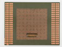
This is a naked IBM Thermal Conduction Module (TCM) substrate, entirely stripped of its iconic helium-filled cooling hat and missing a majority of its silicon. Visually, it is an absolute masterpiece of Cold War-era heavy iron engineering.
The gold brazed sealing ring around the perimeter is flawless and designed to be hermetically sealed against a massive water-cooled block. Looking closely at the top surface, you can see the incredibly intricate footprint of the C4 (Controlled Collapse Chip Connection) flip-chip pads. Only a handful of the logic and array dies are actually populated on this specific unit, forming an incomplete geometric cluster.
Here are the exact identifiers I pulled off the surface and the gold rim:
Gold Ring Engraving: A58495
Ceramic Surface Markings (Left Edge): 74543 349
Ceramic Surface Markings (Right Edge): 69 56132
Ceramic Orientation Marks: +, L, >
When looking at the back of this board, the forest of 1,800 brazed gold pins is staggering. They are immaculate and rigidly aligned. It is a striking contrast to modern socketed CPUs. The sheer amount of precious metal used just in the interconnects and sealing ring makes it obvious why so many of these were mercilessly destroyed by scrap recyclers.
To understand the insanity of the IBM 3081 TCM, you have to look past the visible surface. This 90mm by 90mm white block is not just a carrier. It is an extremely complex multi-layer printed circuit made out of ceramic. Inside this exact piece of alumina, there are up to 33 distinct layers of molybdenum wiring. If you stripped away the ceramic and laid out the internal traces end to end, you would find over 130 meters of microscopic wiring routing power and signals between the 121 possible chip sites.
The bare silicon chips you see on the surface are mounted face-down using IBM's pioneering flip-chip technology. Instead of wire bonding the edges of the silicon, the entire face of the die is covered in tiny solder bumps that mate directly with the gold pads visible on the empty squares. This allowed for massive I/O counts per chip and drastically reduced signal delay.
The thermal challenges here were monumental. In a fully assembled unit, a massive aluminum hat would be bolted over this sealing ring. Inside that hat, spring-loaded metallic pistons would press directly against the back of each one of these bare silicon dies. The entire void inside the module was then pumped full of helium gas to bridge the microscopic gaps between the silicon and the pistons, transferring the immense heat up into a chilled water jacket. It was an incredibly exotic, brute-force solution to keep bipolar emitter-coupled logic (ECL) from melting itself down.
The introduction of the TCM with the System/370 architecture in 1980 changed the mainframe landscape forever. Before this, mainframe logic was spread out over massive, sprawling printed circuit boards which introduced terrible latency. By shrinking the entire CPU complex down onto a few of these dense ceramic tiles, IBM drastically shortened the physical distance signals had to travel.
There is a persistent myth in the vintage hardware community that the helium inside these modules was used for active cryogenic cooling. That is entirely false. The helium was strictly static, chosen purely for its excellent thermal conductivity compared to air. It acted as a gap-filler to ensure the heat transferred efficiently into the mechanical pistons.
Sadly, the legacy of the TCM is also one of mass destruction. Because these units contain massive amounts of high-karat gold in the pins, sealing rings, and internal vias, scrappers actively hunted them down throughout the 1990s and 2000s. Smashing them with hammers to extract the precious metals was standard practice, making surviving naked substrates like this one exceedingly rare.
Identifying this exact piece requires reading the physical clues embedded in the ceramic.
First, I measured the substrate via the provided scale and visual references. It is exactly 90mm by 90mm. Second, I counted the die pad grid. It is an 11 by 11 grid yielding 121 total potential chip sites. These two metrics definitively identify it as an IBM 3081 generation substrate. The later 3090 generation modules were significantly larger and held over 100 chips on a much wider grid.
The most fascinating aspect of this artifact is its incomplete state. Only about 29 of the 121 chip sites are populated with bare silicon. Furthermore, the massive external cooling assembly was never attached, or it was perfectly cleanly removed without tearing the delicate flip-chips off their solder bumps.
Given the hand-engraved A58495 on the gold sealing ring, I strongly suspect this unit was an internal test article, an engineering prototype, or a yield failure that was pulled from the assembly line before being finalized. Fully functional units out in the wild are almost always fully populated and sealed. The fact that we can see the bare C4 solder grids right next to mounted flip-chips makes this a perfect museum piece for demonstrating IBM's bleeding-edge packaging technology.