When I first placed this specific unit on the scale to catalog it for the archive, it registered a hefty 72.3 grams. Holding this piece under the macro lens reveals a fascinating story of high-end industrial hardware and brutal e-waste recycling. This is not just a loose processor. It is a multi-chip module permanently fused to a chunk of its original host system.
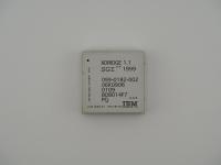
Here is the exact transcription of the laser etching on the metal heatspreader:
IBM
PowerPC (TM)
MCM
PPC603e - 100 MHz
85H1212     9944
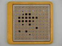
Looking closely at the physical materials, the top layer is a thick, brushed aluminum cap designed to conduct heat away from the silicon into a larger passive chassis. Beneath that cap sits a massive, dark purple ceramic substrate. If you look at the side profiles, you can see faint purple ink stamped directly onto the edge of the ceramic reading BH09881.
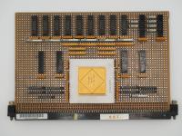
However, the most striking visual detail is the bottom layer. The green FR4 fiberglass is not part of the CPU package. This artifact is a CBGA (Ceramic Ball Grid Array) that is still soldered to the original motherboard. In the macro profile shots, you can clearly see the tiny spherical solder balls bridging the gap between the dark ceramic and the green PCB. The edges of this green board are frayed, jagged, and violently sheared. We can even see a white silkscreen label R333 on the bottom, which designates a surface-mount resistor location on the host board. A recycler literally took a Dremel or a rotary saw and cut this CPU straight out of the motherboard rather than attempting a complex desoldering process.
The PowerPC 603e was a marvel of mid-90s RISC architecture. Co-developed by the AIM alliance (Apple, IBM, and Motorola), the core features roughly 2.6 million transistors built on a 0.5-micron fabrication node. It operates at 100 MHz, which was quite respectable for its original release window.
What makes this specific artifact so technically compelling is the MCM designation. Multi-Chip Modules are essentially microscopic motherboards enclosed within a single package. A standard 603e core does not require a ceramic footprint this massive. The presence of the MCM label and the huge CBGA footprint strongly suggests that IBM integrated supplementary silicon directly onto the ceramic alongside the main CPU die. In industrial and telecom applications, this extra silicon usually took the form of integrated L2 cache SRAM chips or a dedicated system bus bridge (like the IBM 105 PCI bridge). By packing the CPU and the chipset into a single sealed unit, engineers could drastically save board space and improve signal integrity in harsh environments.
The PowerPC 603 family has a dramatic history. When Apple first transitioned to PowerPC, they relied on the original 603 chip for their consumer Macintosh lines. It was a disaster. The original 603 had a tiny L1 cache, and because the Mac OS had to run older software via a 68k emulator, the emulator's code constantly fell out of the tiny cache. Performance tanked.
The 603e (the "e" standing for enhanced) was the emergency fix. IBM and Motorola quadrupled the L1 cache to 32KB total (16KB instruction and 16KB data). This single architectural tweak saved the low-end Macintosh lineup and restored the reputation of the PowerPC architecture.
While Apple fans remember the 603e from their childhood Performa desktops and PowerBook laptops, IBM was quietly making a fortune selling these chips to the enterprise sector. The 603e was legendary for its low power consumption and high reliability. Because of this, it became the undisputed king of embedded 1990s hardware. You would find these powering high-end Cisco enterprise routers, military avionics, automotive controllers, and telecom switching gear.
Researching the exact origins of this chopped-up board requires a bit of forensic deduction. The date code 9944 located on the bottom right of the metal cap indicates this chip was manufactured in the 44th week of 1999.
By late 1999, a 100 MHz processor was completely obsolete for consumer desktop computers. The world had already moved on to the Pentium III and the PowerPC G4. Therefore, I can authoritatively state that this was an embedded component meant for industrial or telecom infrastructure. The lifespan of embedded telecom gear is often decades long. Equipment manufacturers will lock in a hardware contract for a stable, proven chip like the 100 MHz 603e and continue ordering it for five to ten years after its initial consumer release.
The exact IBM part number 85H1212 does not map to any public consumer datasheet. This is incredibly common with enterprise IBM hardware, as these MCMs were often built as custom orders for specific networking clients. Given the brutal extraction method where the board was simply sawed off, it is highly likely this was pulled from a massive rack-mounted telecom switch or an industrial control unit during a corporate e-waste liquidation. The scrappers knew the gold and ceramic in the MCM had value, but the massive multi-layer PCB was too much of a hassle to cleanly desolder.